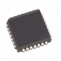
DS2176Q Maxim Integrated Products, DS2176Q Datasheet

DS2176Q
Specifications of DS2176Q
Available stocks
Related parts for DS2176Q
DS2176Q Summary of contents
Page 1
... Integration feature “debounces” signaling § Slip–compensated output indicates when signaling updates occur § Compatible with DS2180A T1 Transceiver § Surface mount package available, designated DS2176Q § Industrial temperature range of –40°C to +85°C available, designated DS2176N DESCRIPTION The DS2176 is a low–power CMOS device specifically designed for synchronizing receive side loop– ...
Page 2
DS2176 BLOCK DIAGRAM Figure DS2176 ...
Page 3
PIN SYMBOL TYPE 1 I SIGN 2 RMSYNC I 3 RCLK I 4 RSER SCHCLK O 10 SM0 I 11 SM1 12 V – ...
Page 4
OVERVIEW The DS2176 performs two primary functions: 1) synchronization of received T1 PCM data (looped timed) to host backplane frequencies; 2) supervision of robbed–bit signaling data embedded in the data stream. The buffer, while optimized for use with the DS2180A ...
Page 5
SSER immediately after the rising edge of the system side frame sync. The F–bit is dropped in 2.048 MHz applications and the MSB of channel 1 appears at SSER one bit period ...
Page 6
SYSTEM MULTIFRAME BOUNDARY TIMING (SYSCLK = 2.048 MHz) Figure 4 193S SYSTEM MULTIFRAME TIMING Figure 5 193E SYSTEM MULTIFRAME TIMING Figure DS2176 ...
Page 7
SIGNALING SUPERVISION EXTRACTION In digital channel banks, robbed–bit signaling data is inserted into the LSB position of each channel during signaling frames. In 193S framing (FMS=0) applications, A signaling data is inserted into frame 6 and B signaling data is ...
Page 8
SIGNALING SUPERVISION MODES Table 2 SM0 SM1 FMS NOTE: 1. During slip or alarm ...
Page 9
DS2176/DS2180A SYSTEM APPLICATION Figure 8 shows how the DS2180A T1 Transceiver and DS2176 Receive Buffer interconnect in a typical application. SERIAL 1.544 MHz BACKPLANE INTERFACE Figure DS2176 ...
Page 10
ABSOLUTE MAXIMUM RATINGS* Voltage on Any Pin Relative to Ground Operating Temperature Storage Temperature Soldering Temperature *This is a stress rating only and functional operation of the device at these or any other conditions above those indicated in the operation ...
Page 11
AC ELECTRICAL CHARACTERISTICS PARAMETERS SYMBOL RCLK Period RCLK, SYSCLK Rise and Fall Times RCLK Pulse Width SYSCLK Pulse Width t SYSCLK Period SYSCLK RMSYNC Setup to RCLK Falling SFSYNC Setup to SYSCLK Falling RMSYNC, SFSYNC, , Pulse Width SIGH ALN ...
Page 12
RECEIVE AC DIAGRAM Figure 9 SYSTEM AC TIMING DIAGRAM Figure DS2176 ...
Page 13
DS2176 T1 RECEIVE BUFFER PKG 24-PIN DIM MIN MAX A IN. 1.245 1.265 MM B IN. 0.250 0.270 MM C IN. 0.125 0.145 MM D IN. 0.300 0.325 MM E IN. 0.015 0.040 MM F IN. 0.125 ...
Page 14
... DS2176Q INCHES DIM MIN A 0.165 A1 0.090 A2 0.020 B 0.026 B1 0.013 C 0.009 D 0.485 D1 0.450 D2 0.390 E 0.485 E1 0.450 E2 0.390 L1 0.060 0.050 BSC CH1 0.042 MAX 0.180 0.120 - 0.033 0.021 0.012 0.495 0.456 0.430 0.495 0.456 0.430 - - 0.048 DS2176 ...
Page 15
DATA SHEET REVISION SUMMARY The following represent the key differences between 04/19/95 and 06/13/97 version of the DS2176 data sheet. Please review this summary carefully. 1. SYNC/CLOCK Relationship in timing diagram DS2176 ...


