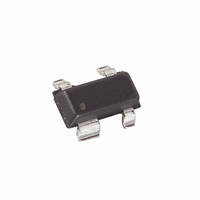
MAX6816EUS+T Maxim Integrated Products, MAX6816EUS+T Datasheet - Page 7

MAX6816EUS+T
Manufacturer Part Number
MAX6816EUS+T
Description
IC DEBOUNCER SWITCH SGL SOT143-4
Manufacturer
Maxim Integrated Products
Datasheet
1.MAX6816EUST.pdf
(8 pages)
Specifications of MAX6816EUS+T
Applications
*
Interface
*
Voltage - Supply
*
Package / Case
SOT-143, SOT-143B, TO-253AA
Mounting Type
Surface Mount
Supply Voltage Range
2.7V To 5.5V
Power Dissipation Pd
320mW
Operating Temperature Range
-40°C To +85°C
Digital Ic Case Style
SOT-143
No. Of Pins
4
Filter Terminals
SMD
Rohs Compliant
Yes
Lead Free Status / RoHS Status
Lead free / RoHS Compliant
meets Level 4 (the highest level) of IEC 1000-4-2, with-
out the need for additional ESD-protection compo-
nents.
The major difference between tests done using the
Human Body Model and IEC 1000-4-2 is higher peak
current in IEC 1000-4-2, because series resistance is
lower in the IEC 1000-4-2 model. Hence, the ESD with-
stand voltage measured to IEC 1000-4-2 is generally
lower than that measured using the Human Body
Model. Figure 7a shows the IEC 1000-4-2 model and
Figure 7b shows the current waveform for the 8kV,
IEC 1000-4-2, Level 4, ESD Contact-Discharge test.
The Air-Gap test involves approaching the device with
a charged probe. The Contact-Discharge method
connects the probe to the device before the probe is
energized.
SUBSTRATE CONNECTED TO GND
PROCESS: BiCMOS
___________________Chip Information
TOP VIEW
±15kV ESD-Protected, Single/Dual/Octal,
_______________________________________________________________________________________
GND
IN1
IN2
1
2
3
SOT23-6
MAX6817
6
5
4
OUT1
V
OUT2
CC
CMOS Switch Debouncers
The Machine Model for ESD tests all pins using a
200pF storage capacitor and zero discharge resis-
tance. Its objective is to emulate the stress caused by
contact that occurs with handling and assembly during
manufacturing.
The MAX6818 has an output enable (EN) input that
allows switch outputs to be three-stated on the µP data
bus until polled by the µP. Also, state changes at the
switch inputs are detected, and an output (CH) goes low
after the debounce period to signal the µP. Figure 4
shows the timing diagram for enabling outputs and read-
ing data. If the output enable is not used, tie EN to GND
to “always enable’’ the switch outputs. If EN is low, CH is
always high. If a change of state is not required, leave
CH unconnected.
For the latest package outline information and land patterns, go
to www.maxim-ic.com/packages. Note that a “+”, “#”, or “-” in
the package code indicates RoHS status only. Package draw-
ings may show a different suffix character, but the drawing per-
tains to the package regardless of RoHS status.
PACKAGE
4 SOT143
20 SSOP
6 SOT23
TYPE
Pin Configurations (continued)
GND
IN1
IN2
IN3
IN4
IN5
IN6
IN7
IN8
EN
10
PACKAGE
1
2
3
4
5
6
7
8
9
CODE
A20-1
U4-1
U6-4
Package Information
MAX6818
SSOP
MAX6818 µP Interfacing
OUTLINE
21-0052
21-0058
21-0056
NO.
20
19
18
17
16
15
14
13
12
11
V
OUT2
OUT3
OUT4
OUT5
OUT6
OUT7
OUT8
CH
OUT1
CC
Machine Model
PATTERN NO.
90-0183
90-0175
90-0094
LAND
7


