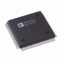
AD9887AKS-140 Analog Devices Inc, AD9887AKS-140 Datasheet - Page 32

AD9887AKS-140
Manufacturer Part Number
AD9887AKS-140
Description
IC INTRFACE ANALOG/DVI 160-MQFP
Manufacturer
Analog Devices Inc
Datasheet
1.AD9887AKSZ-100.pdf
(40 pages)
Specifications of AD9887AKS-140
Rohs Status
RoHS non-compliant
Applications
Graphic Cards, VGA Interfaces
Interface
Analog and Digital
Voltage - Supply
3.15 V ~ 3.45 V
Package / Case
160-MQFP, 160-PQFP
Mounting Type
Surface Mount
Available stocks
Company
Part Number
Manufacturer
Quantity
Price
Company:
Part Number:
AD9887AKS-140
Manufacturer:
AD
Quantity:
275
Company:
Part Number:
AD9887AKS-140
Manufacturer:
TOS
Quantity:
160
Company:
Part Number:
AD9887AKS-140
Manufacturer:
AD
Quantity:
586
Part Number:
AD9887AKS-140
Manufacturer:
ADI/亚德诺
Quantity:
20 000
AD9887
0F
0F
0F
MODE CONTROL 2
10
The default for this register is 0, not inverted.
10
2 Red Clamp Select
1 Green Clamp Select
0 Blue Clamp Select
7 Clk Inv Data Output Clock Invert
A Logic 1 enables the external CKEXT input pin. In this
mode, the PLL Divide Ratio (PLLDIV) is ignored. The
clock phase adjust (PHASE) is still functional.
The power-up default value is EXTCLK = 0.
A bit that determines whether the red channel is clamped
to ground or to midscale. For RGB video, all three chan-
nels are referenced to ground. For YcbCr (or YUV), the
Y channel is referenced to ground, but the CbCr channels
are referenced to midscale. Clamping to midscale actually
clamps to Pin 118, R
Clamp
0
1
The default setting for this register is 0.
A bit that determines whether the green channel is clamped
to ground or to midscale.
Clamp
0
1
The default setting for this register is 0.
A bit that determines whether the blue channel is clamped
to ground or to midscale.
Clamp
0
1
The default setting for this register is 0.
A control bit for the inversion of the output data clocks,
(Pins 134, 135). This function works only for the digital
interface. When not inverted, data is output on the rising
edge of the data clock. See timing diagrams to see how
this affects timing.
Clk Inv
0
1
6 Pix Select
This bit selects either 1 or 2 pixels per clock mode for the
digital interface. It determines whether the data comes out
Table XXV. Clock Output Invert Settings
Table XXIV. Blue Clamp Select Settings
Table XXIII. Green Clamp Select Settings
Table XXII. Red Clamp Select Settings
Function
Clamp to Ground
Clamp to Midscale (Pin 99)
Function
Not Inverted
Inverted
Clamp to Ground
Clamp to Midscale (Pin 109)
Function
Function
Clamp to Ground
Clamp to Midscale (Pin 118)
CLAMP
V.
10
10
10
of a single port (even port only), at the full data rate or
out of two ports (both even and odd ports), at one-half
the full data rate per port. A Logic 0 selects 1 pixel per
clock (even port only). A Logic 1 selects 2 pixels per clock
(both ports). See the Digital Interface Timing Diagrams,
Figures 29 to 32, for a visual representation of this function.
Note: This function operates exactly like the DEMUX
function on the analog interface.
Pix Select
0
1
The default for this register is 0, 1 pixel per clock.
5, 4 Output Drive
These two bits select the drive strength for the high-speed
digital outputs (all data output and clock output pins).
Higher drive strength results in faster rise/fall times and in
general makes it easier to capture data. Lower drive strength
results in slower rise/fall times and helps to reduce EMI
and digitally generated power supply noise. The exact
timing specifications for each of these modes are specified
in Table VII.
Bit 5
1
1
0
The default for this register is 11, high drive strength. (This
option works on both the analog and digital interfaces.)
3 P
A bit that can put the outputs in a high impedance mode.
This applies only to the 48 data output pins and the two
data clock output pins.
Table XXVIII. Power-Down Output Settings
CKINV
0
1
The default for this register is 0. (This option works on
both the analog and digital interfaces.)
2 Sync Detect Polarity
This pin controls the polarity of the Sync Detect output
pin (Pin 136).
Table XXIX. Sync Detect Polarity Settings
Polarity
0
1
The default for this register is 0. (This option works on
both the analog and digital interfaces.)
Table XXVII. Output Drive Strength Settings
DO
Table XXVI. Pix Select Settings
—Power-Down Outputs
Bit 4
1
0
X
Function
1 Pixel per Clock
2 Pixels per Clock
Function
Normal Operation
Three-State
Function
Activity = Logic 1 Output
Activity = Logic 0 Output
Result
High Drive Strength
Medium Drive Strength
Low Drive Strength


