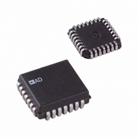
AD7569KP Analog Devices Inc, AD7569KP Datasheet - Page 15

AD7569KP
Manufacturer Part Number
AD7569KP
Description
IC I/O PORT 8BIT ANLG 28-PLCC
Manufacturer
Analog Devices Inc
Series
LC²MOSr
Datasheet
1.AD7569JRZ.pdf
(20 pages)
Specifications of AD7569KP
Rohs Status
RoHS non-compliant
Applications
Analog I/O
Interface
Bus
Voltage - Supply
4.75 V ~ 5.25 V
Package / Case
28-LCC (J-Lead)
Mounting Type
Surface Mount
Converter Type
ADC/DAC
Resolution
8b
Number Of Dac's
Single
Data Rate
0.5MSPS
Digital Interface Type
Parallel
Pin Count
28
Package Type
PLCC
Lead Free Status / Rohs Status
Not Compliant
an RD pulse for the AD7569/AD7669. This RD pulse accesses
data from the ADC and places the conversion result into a regis-
ter on the 74646. The rising edge of this pulse generates an in-
terrupt request to the processor. The conversion result is read
from the 74646 register by performing an I/O read to the
decoded address of the 74646. Writing data to the relevant
AD7569/AD7669 DAC involves an I/O write to the 74646,
which transfers the data to the data inputs of the AD7569/
AD7669. Data is latched into the selected DAC register on the
rising edge of IOW.
APPLYING THE AD7569/AD7669 DAC
An internal gain/offset network on the AD7569/AD7669 allows
several output voltage ranges. The part can produce unipolar
output ranges of 0 V to +1.25 V or 0 V to +2.5 V and bipolar
output ranges of –1.25 V to +1.25 V or –2.5 V to +2.5 V. Con-
nections for these various output ranges are outlined below.
UNIPOLAR (0 V to +1.25 V) CONFIGURATION
The first of the configurations provides an output voltage range
of 0 V to +1.25 V. This is achieved by tying the V
RANGE inputs to AGND
figuration of the AD7569 to achieve this output range. A similar
configuration of the AD7669 gives the same output range. The
table for output voltage versus the digital code in the DAC regis-
ter is shown in Table IV.
DAC Register Contents
MSB LSB
1111
1000
1000
0111
0000
0000
NOTE: 1 LSB = (V
REV. B
Figure 21. AD7569 Unipolar (0 V to +1.25 V) Operation
Table IV. Unipolar (0 V to +1.25 V) Code Table
1111
0001
0000
1111
0001
0000
REF
) (2
–8
) = V
DAC
REF
Analog Output, V
+V
+V
+V
+V
+V
0 V
(= 0 V). Figure 21 shows the con-
(1/256); V
REF
REF
REF
REF
REF
127
256
256
129
128
255
256
256
256
REF
1
= +1.25 V Nominal
= +V
OUT
REF
SS
/2
and
–15–
UNIPOLAR (0 V to +2.5 V) CONFIGURATION
The 0 V to +2.5 V output voltage range is achieved by tying V
to AGND
for output voltage versus digital code is as in Table IV with
2.V
BIPOLAR (–1.25 V to +1.25 V) CONFIGURATION
The first of the bipolar configurations is achieved by tying the
RANGE input to AGND
voltage level at which the AD7569/AD7669 changes to bipolar
operation is approximately –1 V. When the part is configured
for bipolar outputs, the input coding becomes twos comple-
ment. The table for output voltage versus the digital code in the
DAC register is shown in Table V. Note as with the unipolar
configuration, a digital input code of all 0s produces an output
of 0 V. It should be noted, however, that a low pulse on the
RESET line for the bipolar ranges sets the output voltage to
negative full scale.
DAC Register Contents
MSB
0111
0000
0000
1111
1000
1000
NOTE: 1 LSB = (V
BIPOLAR (–2.5 V to +2.5 V) CONFIGURATION
The –2.5 V to +2.5 V bipolar output range is achieved by tying
the RANGE input to V
again, the input coding is 2s complement. The table for output
voltage versus digital code is as in Table V with 2.V
V
REF
REF
. Note that for this range
Table V. Bipolar (–1.25 V to +1.25 V) Code Table
replacing V
LSB
1111
0001
0000
1111
0001
0000
DAC
(= 0 V) and the RANGE input to V
1 LSB
1 LSB
REF
)(2
REF
–7
. Note that for this range
) = V
DD
2.V
DAC
4.V
REF
and the V
REF
(= 0 V) and V
REF
(1/128)
(2
Analog Output, V
+V
+V
0 V
–V
–V
–V
(2
AD7569/AD7669
8
REF
REF
REF
REF
REF
8
) V
SS
) V
input to –5 V. Once
128
127
128
128
128
128
127
128
REF
REF
1
1
SS
128
to –5 V. The V
64
1
1
= –V
DD
OUT
REF
REF
. The table
replacing
SS
SS


