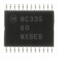
MC33560DTBR2G ON Semiconductor, MC33560DTBR2G Datasheet - Page 4

MC33560DTBR2G
Manufacturer Part Number
MC33560DTBR2G
Description
IC INTERFACE PWR MANAGMT 24TSSOP
Manufacturer
ON Semiconductor
Datasheet
1.MC33560DTBR2.pdf
(26 pages)
Specifications of MC33560DTBR2G
Applications
*
Interface
*
Voltage - Supply
*
Package / Case
24-TSSOP
Mounting Type
Surface Mount
Lead Free Status / RoHS Status
Lead free / RoHS Compliant
Other names
MC33560DTBR2GOS
Available stocks
Company
Part Number
Manufacturer
Quantity
Price
Company:
Part Number:
MC33560DTBR2G
Manufacturer:
ON
Quantity:
142
Part Number:
MC33560DTBR2G
Manufacturer:
ON/安森美
Quantity:
20 000
ELECTRICAL CHARACTERISTICS (continued)
integrated circuits. The convention considers current flowing into the pin (sink current) as positive and current flowing out of the pin
(source current) as negative. (Conditions: V
≤ 85°C, L
APPLICATION INTERFACE DC SECTION (V
CARD INTERFACE DC SECTION (V
DIGITAL DYNAMIC SECTION (V
4. See Figures 2 and 3.
5. The transistors T1 on lines IO, C4 and C8 (see Figure 24) have a max R
6. Pin loading = 30 pF, except INVOUT = 15 pF.
7. As the clock buffer is optimized for low power consumption and hence not symmetrical, clock signal duty cycle is guaranteed for divide
8. In either direction.
Input High Threshold Voltage
(increasing)
Input Low Threshold Voltage
(decreasing)
Switching Hysteresis
Threshold Voltage
Pulldown resistance
Pullup resistance
Output High Voltage
Output Low Voltage
Input Leakage Current
Output High Voltage
Output Low Voltage
I/O Pullup Resistance, Operating
Mode, CS =L , PWRON = H
Card pins security voltage
(Card access deactivated)
Input Clock Frequency
Card Clock Frequency
Card Clock Duty Cycle (Note 7)
Card Clock Rise and Fall Time
I/O Data Transfer Frequency
I/O Duty Cycle
I/O Rise and Fall Time
I/O Transfer Time
Card Signal Sequence Interval
by 2 and divide by 4 ratio.
1
= 47 mH, R
Characteristic
LIM
= 0 W, CRDV
BAT
BAT
= 5.0 V, Normal Operating Mode) (Note 6)
CC
= 5.0 V)
I
Pin [7, 11], [21, 16], [20, 19] (Note 8)
Pin [7, 11], [21, 16], [20, 19] (Note 8)
Pin [7, 11], [21, 16], [20, 19] (Note 8)
Pin [7, 11], [21, 16], [20, 19] (Note 8)
capacitor = 10 mF, unless otherwise noted.)
OH
V
BAT
50% to 50% V
IN
PWRON = GND, lin = 10 mA,
= −2.5 mA, Pin 3, Pin 4 for CS = H
I
I
I
OH
BAT
OL
V
I
OL
V
= V
OH
Pin 15, 50% to 50% V
I
I
I
Pin 15, 10% ↔ 90% V
= 4.0 V, V
OL
Pin 9, Duty Cycle = 50%
CC
OL
OL
OL
Pin 4 ( in Output Mode)
V
Pins 11, 14, 15, 16, 19
Pins 11, 14, 15, 16, 19
= 1.0 mA, Pins 11, 16, 19
Pins 2, 4, 5, 6, 10, 17
Pins 2, 4, 5, 6, 10, 17
Pins 9, 17, 18, 20, 21
= −20 mA, Pins 11, 16, 19
= 1.0 mA, Pins 7, 20, 21
I
V
BAT
= 5.0 V)
IN
= −50 mA, pins 7, 20,21
OH
= 0.5 V, Pins 11, 16, 19
= 0.2 mA, Pins 3, 4, 8
= 0.2 mA, Pins 14, 15
= 0.2 mA, Pins 14, 15
Powerup / Powerdown
IN
10% ↔ 90% V
Test Conditions
50% to 50% V
Pins 2, 5, 6, 10
= 0.5 V, Pin 3, 4, 5
= −0.2 mA, Pin 8
= 2.5 V, CS = H,
f
− 1.0 V, Pins 2, 6, 7, 10
io
These specifications are written in the same style as common for standard
= 16 MHz
Pin 17
Pin 18
Pin 15
CC
Pin 4
Pin 9
http://onsemi.com
CC
= 5.0 V nom, PWRON = V
, L → H, H → L
MC33560
CC
CC
4
CC
CC
,
dson
of 250 W.
Symbol
V
t
rclk
V
t
R
f
±I
f
rio
security
asyclk
t
V
V
crdclk
V
V
V
R
V
HYST
dseq
V
r
down
r
f
leak
clk
t
OH
OH
−
TH
OL
OL
, t
, t
io
io
IH
up
tr
BAT
IL
fclk
fio
, Operating Mode, −I
0.55*V
0.06*V
V
0.3*V
0.2*V
0.3*V
0.5*V
0.4*V
V
CC
BAT
Min
120
120
45
45
−
−
−
−
−
−
−
−
−
−
−
−
− 0.9
BAT
BAT
BAT
BAT
BAT
− 1
BAT
BAT
Typ
240
240
1.0
0.2
18
−
−
−
−
−
−
−
−
−
−
−
−
−
−
−
−
−
−
−
−
CC
= 10 mA, −25°C ≤ T
0.65*V
0.45*V
0.40*V
0.5*V
0.3*V
0.6*V
0.6*V
Max
500
500
150
100
0.4
2.0
0.4
2.0
1.0
20
20
55
10
55
−
−
−
−
BAT
BAT
BAT
BAT
BAT
BAT
BAT
Unit
MHz
MHz
MHz
kW
kW
kW
mA
ns
ns
ns
ms
%
%
V
V
V
V
V
V
V
V
V
A


