ADG509AKNZ Analog Devices Inc, ADG509AKNZ Datasheet - Page 9
ADG509AKNZ
Manufacturer Part Number
ADG509AKNZ
Description
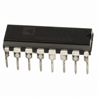
IC MULTIPLEXER DUAL 4X1 16DIP
Manufacturer
Analog Devices Inc
Specifications of ADG509AKNZ
Function
Multiplexer
Circuit
2 x 4:1
On-state Resistance
300 Ohm
Voltage Supply Source
Dual Supply
Voltage - Supply, Single/dual (±)
±10.8 V ~ 16.5 V
Current - Supply
20µA
Operating Temperature
-40°C ~ 85°C
Mounting Type
Through Hole
Package / Case
16-DIP (0.300", 7.62mm)
No. Of Circuits
2
Supply Current
600µA
On State Resistance Max
280ohm
Supply Voltage Range
10.8V To 16.5V
Operating Temperature Range
-40°C To +85°C
Analog Switch Case Style
DIP
Lead Free Status / RoHS Status
Lead free / RoHS Compliant
Lead Free Status / RoHS Status
Lead free / RoHS Compliant, Lead free / RoHS Compliant
Available stocks
Company
Part Number
Manufacturer
Quantity
Price
Company:

Part Number:
ADG509AKNZ
Manufacturer:
ADI
Quantity:
36
Part Number:
ADG509AKNZ
Manufacturer:
ADI/亚德诺
Quantity:
20 000


Table 6. ADG509A Pin Function Description
DIP/SOIC
1
2
3
4
5
6
7
8
9
10
11
12
13
14
15
16
N/A
N/A
N/A
N/A
Table 7. ADG509A Truth Table
A1
X
0
0
1
1
1
X = don’t care.
1
Pin Number
PLCC/LCC
2
3
4
5
7
8
9
10
12
13
14
15
17
18
19
20
1
6
11
16
S1A
S2A
S3A
S4A
V
DA
EN
A0
SS
Figure 6. ADG509A DIP, SOIC
X
0
1
0
1
A0
1
2
3
4
5
6
7
8
1
X
(Not to Scale)
ADG509A
Mnemonic
A0
EN
V
S1A
S2A
S3A
S4A
DA
DB
S4B
S3B
S2B
S1B
V
GND
A1
NC
NC
NC
NC
TOP VIEW
SS
DD
16
15
14
13
12
11
10
9
A1
GND
V
S1B
S2B
S3B
S4B
DB
Description
Logic Control Input.
Active High Digital Input. When low, the device is disabled and all switches are off.
When high, Ax logic inputs determine on switches.
Most Negative Power Supply Potential in Dual Supplies. In single-supply applications,
it can be connected to ground.
Source Terminal 1A. Can be an input or an output.
Source Terminal 2A. Can be an input or an output.
Source Terminal 3A. Can be an input or an output.
Source Terminal 4A. Can be an input or an output.
Drain Terminal A. Can be an input or an output.
Drain Terminal B. Can be an input or an output.
Source Terminal 4B. Can be an input or an output.
Source Terminal 3B. Can be an input or an output.
Source Terminal 2B. Can be an input or an output.
Source Terminal 1B. Can be an input or an output.
Most Positive Power Supply Potential.
Ground (0 V) Reference.
Logic Control Input.
No Connect.
No Connect.
No Connect.
No Connect.
EN
0
1
1
1
1
DD
Rev. D | Page 9 of 16
On Switch Pair
None
1
2
3
4
S1A
S2A
S3A
V
NC
SS
4
5
6
7
8
3
9
(Not to Scale)
Figure 7. ADG509A PLCC
ADG509A
PIN 1
IDENTIFIER
TOP VIEW
10
2
11
1
20
12
19
13
ADG508A/ADG509A
NC = NO CONNECT
18
17
16
15
14
V
S1B
NC
S2B
S3B
DD
Related parts for ADG509AKNZ
Image
Part Number
Description
Manufacturer
Datasheet
Request
R

Part Number:
Description:
±1.7g Dual-Axis IMEMS Accelerometer Evaluation Board
Manufacturer:
Analog Devices Inc
Datasheet:

Part Number:
Description:
Inertial Sensor Evaluation System
Manufacturer:
Analog Devices Inc
Datasheet:
Part Number:
Description:
Manufacturer:
Analog Devices Inc
Datasheet:
Part Number:
Description:
Manufacturer:
Analog Devices Inc
Datasheet:
Part Number:
Description:
Manufacturer:
Analog Devices Inc
Datasheet:
Part Number:
Description:
Manufacturer:
Analog Devices Inc
Datasheet:
Part Number:
Description:
Manufacturer:
Analog Devices Inc
Datasheet:
Part Number:
Description:
Manufacturer:
Analog Devices Inc
Datasheet:
Part Number:
Description:
Manufacturer:
Analog Devices Inc
Datasheet:
Part Number:
Description:
Manufacturer:
Analog Devices Inc
Datasheet:
Part Number:
Description:
Manufacturer:
Analog Devices Inc
Datasheet:
Part Number:
Description:
Manufacturer:
Analog Devices Inc
Datasheet:
Part Number:
Description:
Manufacturer:
Analog Devices Inc
Datasheet: