BCS2015A1 TDK Corporation, BCS2015A1 Datasheet
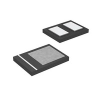
PHOTODIODE VISIBLE 2X1.5MM SMD

BCS2015A1

Manufacturer Part Number
BCS2015A1
Description
PHOTODIODE VISIBLE 2X1.5MM SMD
Manufacturer
TDK Corporation
Type
Photodioder
Datasheet

Specifications of BCS2015A1

Wavelength
580nm
Output Type
Current On Typ, 8µA
Package / Case
0806 (2015 Metric)
Lead Free Status / Rohs Status
Lead free / RoHS Compliant
Other names
445-2592-2
TDK Visible Radiant Optical Sensor is the photo-IC which uses an amorphous
silicone semiconductor technology.  It is the most suitable for Brightness
Adjustment, Control of the Lighting systems. BCS2015A1 has current-
amplifire in it. BCS2015A1 is for surface mounthing.
Features
• Highly receptive to visible light but not receptive to infrared light (close to
Human eye visibility).
• Accurate illumination measurement can be taken without the use of an
infrared filter.
( Phototransistors and photodiodes that use crystal- silicon semiconductors
typically require this filtering.)
• High output (Built-in current amplifire)
• Surface mounting can be used in lead- free reflow soldering.
• Lead- free, Cadmium-free
Dimensions in [mm]
( ) : Typical value
Shapes and dimension
Glass Substrate
BCS2015A1
*All specifications are subject to change without notice.
Visible Radiant Optical Sensor /Data Sheet
Electrical Characterisic
Output current
Operation voltage (Vop)
Dark current
Absolute Maximum Ratings
Operation voltage
Reverse voltage
Output current
Optical Characteristic
Spectral sensivty area
Peak of sensivity
Others
Operating temperature
Keep and transfer temperature
Dimensions
Weight
(0.55)
*1 White Fluor Light (color temperature=4200K)
(1.325)
2
100Lux*1
Vop=5V
Photo acceptance area
100Lux*1
Item
Item
Item
Item
- Electrode
Vop=5V
0.6
0.5
Application
• Brightness control for LCD, EL and CRT
• Brightness control for Keypads (e. g. Mobile Phones)
• Positioning scanline for Rear Projecton TV
• Exposure adjust for Compact Camera
• Sub exposure adjust for Digital Camera
0.6
+ Electrode
deg. C
deg. C
Units
Units
Units
Units
mm
mA
nm
nm
μA
nA
V
V
V
g
t=0.6(typ.)
0.7(Max.)
Min.
6.0
1.2
---
Value
Value
Value
Value
2.0×1.5×0.6t
350 to 750
580±20
Temperature= 25deg.C
-20 to 85
-40 to 85
Equivalent circuit
0.004
-1
8
1
Typ.
8.0
---
---
*Initial value
BCS2015A1
10.0
Max.
5.0
10
_
+
51101

Related parts for BCS2015A1

BCS2015A1 Summary of contents

Page 1

... Visible Radiant Optical Sensor /Data Sheet TDK Visible Radiant Optical Sensor is the photo-IC which uses an amorphous silicone semiconductor technology.  It is the most suitable for Brightness Adjustment, Control of the Lighting systems. BCS2015A1 has current- amplifire in it. BCS2015A1 is for surface mounthing. Features • Highly receptive to visible light but not receptive to infrared light (close to Human eye visibility). • ...

Page 2

... Output characteristic(typical):BCS2015A1 1.E-02 1.E-03 1.E-04 1.E-05 1.E-06 1.E-07 1 Measuring circuit diagram Light Optical sensor Vop=3V Vop=4V Vop=5V 10 100 1,000 Illuminance(Lx Vop V V-meter - 10,000 100,000 I-meter 2 ...

Page 3

... BCS2015A1 Characteristic of Output Voltage (Typical) Measuring circuit 4.5 4 3.5 3 2.5 2 1.5 1 0.5 0 100 Photo- Illuminance dependency of Max. Vo (Typical) Vcc=5V Vcc=3V 1000 Illuminance(Lx) Vcc 10000 ...

Page 4

Vcc=5V 1.E+00 1.E-01 1.E-02 1.E-03 1.E+00 1.E+01 1.E+01 1.E+00 Vcc=3V 1.E-01 1.E-02 1.E-03 1.E+00 1.E+01 RL=4k ohm RL=55k ohm RL=630k ohm 1.E+02 1.E+03 Illuminamce(Lx) 1.E+02 1.E+03 Illuminance(Lx) 1.E+04 RL=950 ohm RL=20k ohm RL=260k ohm 1.E+04 ...

Page 5

... Typical photo response time:BCS2015A1 (typ.) 1.E-02 1.E-03 1.E-04 1.E+03 Measuring circuit + LED pulse light - Optical sensor tr tf 1.E+04 Load Resistor RL (Ω) 5V Vout Vout RL 1.E+05 2V 90% 10 ...

Page 6

... Temperature stability of output current:BCS2015A1 (typical) 1.2 1.1 1 0.9 0.8 0.7 0.6 -10 0 Spectral response:BCS2015A1 (typical) 1.0 0.8 0.6 0.4 0.2 0.0 300 Temperature(deg.C) Human eyes (CIE standard) 400 500 Wave length(nm) *VR=5V FL 100Lux BCS2015A1 600 700 800 3 ...

Page 7

Recommended land pattern Recommended land pattern is shown in Fig. shown in Fig. to the direction of curvature as the result of heat stress by reflow and/or physical stress. Recommanded reflow heat condition For Pb-Flee soldering process 245deg./C - 255deg./C ...

Related keywords