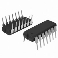
MC74HC4066ANG ON Semiconductor, MC74HC4066ANG Datasheet

MC74HC4066ANG
Specifications of MC74HC4066ANG
Available stocks
Related parts for MC74HC4066ANG
MC74HC4066ANG Summary of contents
Page 1
MC74HC4066A Quad Analog Switch/ Multiplexer/Demultiplexer High−Performance Silicon−Gate CMOS The MC74HC4066A utilizes silicon−gate CMOS technology to achieve fast propagation delays, low ON resistances, and low − ...
Page 2
... State of Input Analog Switch L Off H On ORDERING INFORMATION Device MC74HC4066AN MC74HC4066ANG MC74HC4066AD MC74HC4066ADG MC74HC4066ADR2 MC74HC4066ADR2G MC74HC4066ADTR2 MC74HC4066ADTR2G MC74HC4066AFEL MC74HC4066AFELG †For information on tape and reel specifications, including part orientation and tape sizes, please refer to our Tape and Reel Packaging Specifications Brochure, BRD8011/D. ...
Page 3
... Package) Î Î Î Î Î Î Î Î Î Î Î Î Î Î NOTE: Information on typical parametric values can be found in the ON Semiconductor High−Speed CMOS Data Book (DL129/D). Î Î Î Î Î Î Value Î Î Î Î Î Î ...
Page 4
... For propagation delays with loads other than 50 pF, see the ON Semiconductor High−Speed CMOS Data Book (DL129/D). 2. Information on typical parametric values can be found in the ON Semiconductor High−Speed CMOS Data Book (DL129/D). ...
Page 5
ADDITIONAL APPLICATION CHARACTERISTICS Î Î Î Î Î Î Î Î Î Î Î Î Î Î Î Î Î Î Î Î Î Î Î Î Î Î Î Î Symbol Parameter Î Î Î Î Î Î Î ...
Page 6
V , INPUT VOLTAGE (VOLTS), REFERENCED TO GROUND is Figure 1a. Typical On Resistance, V 200 180 160 140 120 100 0.00 ...
Page 7
V , INPUT VOLTAGE (VOLTS), REFERENCED TO GROUND is Figure 1d. Typical On Resistance ...
Page 8
PROGRAMMABLE V CC GND A OFF V CC SELECTED CONTROL 7 INPUT Figure 3. Maximum Off Channel Leakage Current, Any One Channel, Test Set−Up PLOTTER MINI COMPUTER POWER SUPPLY − + DEVICE UNDER TEST ANALOG IN COMMON OUT GND Figure ...
Page 9
0.1mF SELECTED V CC CONTROL 7 INPUT *Includes all probe and jig capacitance. Figure 5. Maximum On−Channel Bandwidth Test Set− OFF/ON SELECTED CONTROL ≤ 1 MHz V 7 INPUT ...
Page 10
ANALOG IN ANALOG OUT ON SELECTED V CC CONTROL 7 INPUT *Includes all probe and jig capacitance. Figure 9. Propagation Delay Test Set−Up POSITION 1 WHEN TESTING t 2 POSITION WHEN TESTING ...
Page 11
APPLICATION INFORMATION The ON/OFF Control pins should levels, V being recognized as logic high and GND being CC recognized as a logic low. Unused analog inputs/outputs may ...
Page 12
V 14 ANALOG SIGNALS HC4066A LSTTL/ NMOS 5 6 CONTROL INPUTS Using Pull-Up Resistors Figure 18. LSTTL/NMOS to HCMOS Interface ...
Page 13
−T− SEATING PLANE 0.13 (0.005) PACKAGE DIMENSIONS PDIP−14 CASE 646−06 ISSUE http://onsemi.com 13 NOTES: 1. DIMENSIONING AND TOLERANCING PER ANSI ...
Page 14
... G −T− SEATING 14 PL PLANE 0.25 (0.010 14X 0.58 *For additional information on our Pb−Free strategy and soldering details, please download the ON Semiconductor Soldering and Mounting Techniques Reference Manual, SOLDERRM/D. PACKAGE DIMENSIONS SOIC−14 CASE 751A−03 ISSUE 0.25 (0.010 ...
Page 15
... S A −V− C 0.10 (0.004) −T− SEATING G D PLANE 14X 0.36 *For additional information on our Pb−Free strategy and soldering details, please download the ON Semiconductor Soldering and Mounting Techniques Reference Manual, SOLDERRM/D. PACKAGE DIMENSIONS TSSOP−14 CASE 948G−01 ISSUE 0.25 (0.010) ...
Page 16
... Opportunity/Affirmative Action Employer. This literature is subject to all applicable copyright laws and is not for resale in any manner. PUBLICATION ORDERING INFORMATION LITERATURE FULFILLMENT: Literature Distribution Center for ON Semiconductor P.O. Box 5163, Denver, Colorado 80217 USA Phone: 303−675−2175 or 800−344−3860 Toll Free USA/Canada Fax: 303− ...


