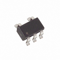
MAX4789EUK+T Maxim Integrated Products, MAX4789EUK+T Datasheet - Page 8

MAX4789EUK+T
Manufacturer Part Number
MAX4789EUK+T
Description
IC SWITCH 1X1 SOT23-5
Manufacturer
Maxim Integrated Products
Datasheet
1.MAX4793EUKT.pdf
(11 pages)
Specifications of MAX4789EUK+T
Function
Switch
Circuit
1 x 1:1
On-state Resistance
400 mOhm
Voltage Supply Source
Single Supply
Voltage - Supply, Single/dual (±)
2.3 V ~ 5.5 V
Current - Supply
80µA
Operating Temperature
-40°C ~ 85°C
Mounting Type
Surface Mount
Package / Case
SC-74A, SOT-753
Lead Free Status / RoHS Status
Lead free / RoHS Compliant
Other names
MAX4789EUK+T
MAX4789EUK+TTR
MAX4789EUK+TTR
200mA/250mA/300mA Current-Limit Switches
To limit the input voltage drop during momentary output
short-circuit conditions, connect a capacitor from IN to
GND. A 0.1µF ceramic capacitor is adequate for most
applications; however, higher capacitor values further
reduce the voltage drop at the input and are recom-
mended for lower voltage applications.
Connect a 0.1µF capacitor from OUT to GND. This
capacitor helps prevent inductive parasitics from
pulling OUT negative during turn-off, thus preventing
Figure 3. MAX4789/MAX4791/MAX4793 Latch-Off Fault
Blanking
8
CURRENT
FLAG PIN
FLAG PIN
VOLTAGE
CURRENT
SWITCH
VOLTAGE
STATUS
STATUS
STATUS
SWITCH
STATUS
_______________________________________________________________________________________
ON PIN
IN PIN
LOAD
LOAD
OFF
OFF
ON
ON
Applications Information
t
BLANK
t
BLANK
UVLO
t
(b)
(a)
BLANK
t
BLANK
Output Capacitance
Input Capacitor
the MAX4789–MAX4794 from tripping erroneously. If
the load capacitance is too large, then current may not
have enough time to charge the capacitance and the
device assumes that there is a faulty load condition.
The maximum capacitive load value that can be driven
from OUT is obtained by the following formula:
To optimize the switch response time to output short-
circuit conditions, it is very important to keep all traces
as short as possible to reduce the effect of undesirable
parasitic inductance. Place input and output capacitors
as close as possible to the device (no more than 5mm).
IN and OUT pins must be connected with short traces
to the power bus.
During normal operation, the power dissipation is small
and the package temperature change is minimal. If the
output is continuously shorted to ground at the maxi-
mum supply voltage, the operation of the switches with
the autoretry option does not cause problems because
the total power dissipated during the short is scaled by
the duty cycle:
where V
t
Attention must be given to the MAX4789, MAX4791,
and MAX4793 where the latch-off condition must be
manually reset by toggling ON from high to low. If the
latch-off time duration is not sufficiently high, it is possi-
ble for the device to reach the thermal-shutdown
threshold and never be able to turn the device on until it
cools down.
PROCESS: BiCMOS
RETRY
P
MAX
= 98ms.
IN
=
C
= 5.5V, I
V
MAX
IN MAX
_
Layout and Thermal Dissipation
<
I
t
FWD MIN
RETRY
OUT
×
I
OUT MAX
_
= 450mA, t
+
_
t
BLANK
Chip Information
×
V
IN
t
BLANK MIN
×
t
BLANK
BLANK
_
=
= 14ms, and
302
mW


