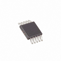
MAX1693EUB+ Maxim Integrated Products, MAX1693EUB+ Datasheet - Page 8

MAX1693EUB+
Manufacturer Part Number
MAX1693EUB+
Description
IC USB SWITCH 1X1 10UMAX
Manufacturer
Maxim Integrated Products
Datasheet
1.MAX1693EUB.pdf
(9 pages)
Specifications of MAX1693EUB+
Function
USB Switch
Circuit
1 x 1:1
On-state Resistance
90 mOhm
Voltage Supply Source
Single Supply
Voltage - Supply, Single/dual (±)
2.7 V ~ 5.5 V
Current - Supply
25µA
Operating Temperature
-40°C ~ 85°C
Mounting Type
Surface Mount
Package / Case
10-MSOP, Micro10™, 10-uMAX, 10-uSOP
Maximum Operating Temperature
+ 85 C
Minimum Operating Temperature
- 40 C
Mounting Style
SMD/SMT
Input Voltage
5.5V
No. Of Outputs
4
Power Dissipation Pd
444mW
Supply Voltage Range
2.7V To 5.5V
No. Of Pins
10
Operating Temperature Range
-40°C To +85°C
Filter Terminals
SMD
Rohs Compliant
Yes
Lead Free Status / RoHS Status
Lead free / RoHS Compliant
The MAX1693/(MAX1693H)/MAX1694 feature 10ms
fault blanking. Fault blanking allows current-limit faults,
including momentary short-circuit faults that occur
when hot-swapping a capacitive load, and also ensures
that no fault is issued during power-up. When a load
transient causes the device to enter current limit, an
internal counter starts. If the load fault persists beyond
the 10ms fault-blanking timeout, the FAULT output
asserts low. Ensure that the MAX1693/(MAX1693H)/
MAX1694’s input is adequately bypassed to prevent
input glitches from triggering spurious FAULT outputs.
Input voltage glitches less than 150mV will not cause a
spurious FAULT output. Load-transient faults less than
10ms (typ) will not cause a FAULT output assertion.
Only current-limit faults are blanked. Die overtempera-
ture faults and input voltage droops below the UVLO
threshold will cause an immediate fault output.
The MAX1694 features a latched FAULT output.
Whenever the FAULT output is activated, it latches the
FAULT output low and also turns the switch off. To clear
the latch, either cycle the ON input or cycle the input
voltage below UVLO.
To limit the input voltage drop during momentary output
short-circuit conditions, connect a capacitor from IN to
GND. A 1µF ceramic capacitor will be adequate for most
applications; however, higher capacitor values will fur-
ther reduce the voltage drop at the input (see Figure 2).
USB Current-Limited Switches
with Fault Blanking
Figure 2. Typical Application Circuit
8 ________________________________________________________________________________________
2.7V TO 5.5V
*USB SPECIFICATIONS REQUIRE A LARGER CAPACITOR
1µF
INPUT
ON
(OFF)
(ON)
OFF
100k
Fault Latching (MAX1694 Only)
Applications Information
IN
FAULT
ON (ON)
(MAX1693H)
MAX1693
MAX1694
GND
OUT
Input Capacitor
Fault Blanking
0.1µF*
OUTPUT
Connect a 0.1µF capacitor from OUT to GND. This cap-
acitor helps prevent inductive parasitics from pulling
OUT negative during turn-off.
To optimize the switch-response time to output short-
circuit conditions, it is very important to keep all traces
as short as possible to reduce the effect of undesirable
parasitic inductance. Place input and output capacitors
as close to the device as possible (no more than 5mm).
All IN and all OUT pins must be connected with short
traces to the power bus. Wide power bus planes will
provide superior heat dissipation through the switch IN
and OUT pins. Figure 3 shows suggested pin connec-
tions for a single-layer board.
Under normal operating conditions, the package can
dissipate and channel heat away. Calculate the maxi-
mum power dissipation as follows:
where I
R
When the output is short-circuited, foldback-current lim-
iting activates and the voltage drop across the switch
equals the input supply. The power dissipated across
the switch increases, as does the die temperature. If the
fault condition is not removed, the thermal-overload-pro-
tection circuitry activates (see the Thermal Shutdown
section). Wide power-bus planes connected to IN and
OUT and a ground plane in contact with the device will
help dissipate additional heat.
TRANSISTOR COUNT: 715
Figure 3. IN and OUT Cross Connections for a Single-Layer
Board
ON
is the on-resistance of the switch (125mΩ max).
LIMIT
1
2
3
4
5
is the preset current limit (1.0A max) and
Layout and Thermal Dissipation
P = (I
OUT
IN
OUT
IN
ON (ON)
(MAX1693H)
MAX1693
MAX1694
LIMIT
Chip Information
)
2
✕
FAULT
GND
OUT
OUT
R
Output Capacitor
IN
ON
10
9
8
7
6


