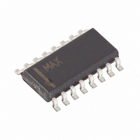
DG202CSE+ Maxim Integrated Products, DG202CSE+ Datasheet - Page 3

DG202CSE+
Manufacturer Part Number
DG202CSE+
Description
IC SWITCH QUAD SPST 16SOIC
Manufacturer
Maxim Integrated Products
Type
Analog Switchr
Datasheet
1.DG202CSE.pdf
(12 pages)
Specifications of DG202CSE+
Function
Switch
Circuit
4 x SPST - NO
On-state Resistance
175 Ohm
Voltage Supply Source
Dual Supply
Voltage - Supply, Single/dual (±)
±4.5 V ~ 18 V
Operating Temperature
0°C ~ 70°C
Mounting Type
Surface Mount
Package / Case
16-SOIC (0.154", 3.90mm Width)
Package
16SOIC N
Maximum On Resistance
200@±15V Ohm
Maximum High Level Output Current
20 mA
Maximum Turn-off Time
450@±15V ns
Maximum Turn-on Time
600@±15V ns
Switch Architecture
SPST
Power Supply Type
Single|Dual
Lead Free Status / RoHS Status
Lead free / RoHS Compliant
ELECTRICAL CHARACTERISTICS (DG202)
(V+ = +15V, V- = -15V, GND = 0, T
ELECTRICAL CHARACTERISTICS (DG212) (continued)
(V+ = +15V, V- = -15V, GND = 0, T
Note 2: Typical values are for DESIGN AID ONLY, not guaranteed nor subject to production testing.
Note 3: I
Note 4: OFF-Isolation = 20 log V
ABSOLUTE MAXIMUM RATINGS (DG202)
Voltages Reference to V-
Digital Inputs (Note 1), V
Current, Any Terminal Except S or D………..….…………...30mA
Continuous Current, S or D…………………………………...20mA
Peak Current, S or D
Note 1: Signals on S
Note 2: Device mounted with all leads soldered to PC board.
Stresses beyond those listed under “Absolute Maximum Ratings” may cause permanent damage to the device. These are stress ratings only, and functional
operation of the device at these or any other conditions beyond those indicated in the operational sections of the specifications is not implied. Exposure to
absolute maximum rating conditions for extended periods may affect device reliability.
SWITCH
Analog Signal Range
Drain-Source ON Resistance
Source OFF-Leakage Current
Drain OFF-Leakage Current
Drain ON-Leakage Current
(Note 4)
SUPPLY
Positive Supply Current
Negative Supply Current
Logic Supply Current
Power-Supply Range
for Continous Operation
V+………………………………………………..……………..44V
GND……………………………………………..……….…….25V
(pulsed at 1ms 10% duty cycle max)…………………….70mA
rent limited to 25mA.
PARAMETER
D(ON)
PARAMETER
is leakage from driver into “ON” switch.
_
_______________________________________________________________________________________
, D
S
_
, or IN
, V
D
............................-2V to (V+ + 2V)
_
or 20mA, whichever occurs first
S
exceeding V+ or V- on Maxim’s DG202 will be clamped by internal diodes, and are also internally cur-
SYMBOL
V
R
/V
A
A
I
I
ANALOG
I
S (OFF)
D (OFF)
DS (ON)
Quad SPST CMOS Analog Switches
D (ON)
D
= +25°C, unless otherwise noted.) (For more information on TYP values see Note 2.)
= +25°C, unless otherwise noted.) (For more information on TYP values see Note 3.)
, V
SYMBOL
S
V
I+
I
I-
OP
L
= input to OFF switch, V
V
V
V
V
D
IN
IN
IN
= ±10V, V
= 0.8V
= 0.8V
= 2.4V
V
IN
= 0 and 2.4V (all)
CONDITIONS
IN
V
V
V
V
V
V
S
S
S
S
S
S
= 2.4V, I
= 14V, V
= -14V, V
= 14V, V
= -14V, V
= -14V
= 14V
CONDITIONS
D
= output.
S
Operating Temperature Range
Storage Temperature Range………………..…..-65°C to +150°C
Power Dissipation (Note 2)
D
D
D
D
= 1mA
= -14V
= -14V
DG202C ....................…………........………..…...0°C to +70°C
DG202D/E............………………….....…..….…-40°C to +85°C
DG202A ..........………........................…….…-55°C to +125°C
16-Pin Plastic Dip (derate 10.5mW/°C above +70°C) ...842mW
16-Pin SO (derate 8.7mW/°C above +70°C) .................696mW
16-Pin TSSOP (derate 9.4mW/°C above +70°C) ...........755mW
16-Pin QFN (5
16-Pin CERDIP (derate 10.0mW/°C above +70°C)......800mW
= 14V
= 14V
(derate 19.2mW/°C above +70°C)...........................1538mW
MIN
-1.0
-1.0
-1.0
-15
✕
DG202A
5)
-0.02
-0.02
TYP
0.01
0.01
115
0.1
±4.5
MIN
MAX
175
1.0
1.0
1.0
15
MIN
-1.0
-1.0
-5.0
-15
TYP
0.02
0.01
DG202C, D, E
0
-0.02
-0.02
TYP
0.01
0.01
115
0.1
±18.0
MAX
0.4
0.4
0
MAX
200
5.0
5.0
1.0
15
UNITS
UNITS
mA
nA
V
Ω
V
3


