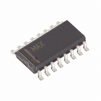
DG211CSE+ Maxim Integrated Products, DG211CSE+ Datasheet - Page 5

DG211CSE+
Manufacturer Part Number
DG211CSE+
Description
IC SWITCH QUAD SPST 16SOIC
Manufacturer
Maxim Integrated Products
Datasheet
1.DG211CSE.pdf
(12 pages)
Specifications of DG211CSE+
Function
Switch
Circuit
4 x SPST - NC
On-state Resistance
175 Ohm
Voltage Supply Source
Dual Supply
Voltage - Supply, Single/dual (±)
±4.5 V ~ 18 V
Operating Temperature
0°C ~ 70°C
Mounting Type
Surface Mount
Package / Case
16-SOIC (0.154", 3.90mm Width)
Number Of Switches
Quad
Switch Configuration
SPST
On Resistance (max)
175 Ohms
On Time (max)
1000 ns
Off Time (max)
500 ns
Off Isolation (typ)
70 dB
Supply Voltage (max)
+/- 18 V
Supply Voltage (min)
+/- 4.5 V
Supply Current
0.02 mA
Maximum Power Dissipation
696 mW
Maximum Operating Temperature
+ 70 C
Mounting Style
SMD/SMT
Description/function
Analog Switch
Input Level
CMOS, TTL
Minimum Operating Temperature
0 C
Off State Leakage Current (max)
5 nA
Lead Free Status / RoHS Status
Lead free / RoHS Compliant
ELECTRICAL CHARACTERISTICS (DG201A)
(V+ = +15V, V- = -15V, GND = 0, T
values see Note 3.)
Switch output waveform shown for V
logic input waveform as shown. Note that V
+ve or -ve as per switching times test circuit. V
steady state output with switch on. Feedthrough via
gate capacitance may result in spikes at leading and
trailing edge of output waveform.
Note 5: Electrical characteristics, such as ON-Resistance, will change when power supplies other than ±15V, are used.
Note 6: I
DIP/SO/TSSOP
SWITCH
Analog Signal Range
D r ai n- S our ce ON Resi stance
( N ote 5)
Source OFF Leakage Current
Drain OFF Leakage Current
Drain ON Leakage
Current (Note 6)
INPUT
Input Current with Input
Voltage High
Input Current with Input
Voltage Low
2, 15, 10, 7
3, 14, 11, 6
1, 16, 9, 8
12
13
4
5
PARAMETER
D (ON)
Switching Time Test Circuit
is leakage from driver into “ON” switch.
PIN
15, 14, 7, 6
16, 13, 8, 5
_______________________________________________________________________________________
1, 12, 9, 4
QFN
10
11
2
3
SYMBOL
V
R
I
I
ANALOG
I
D (OFF)
DS (ON)
S (OFF)
D (ON)
A
Quad SPST CMOS Analog Switches
I
I
INH
INL
= full opearting temperature range, unless otherwise noted.) (For more information on TYP
IN1–IN4
D1–D4
NAME
S1–S4
GND
N.C.
V+
V-
S
V
V
V
V
V
V
V
D
IN
IN
IN
IN
IN
IN
= constant with
= ±10V, V
= 2.4V
= 2.4V
= 0.8V
= 2.4V
= 15V
= 0
Input
Analog Switch Drain Terminal
Analog Switch Source Terminal
Negative-Supply Voltage Input
Ground
No Connection
Positive-Supply Voltage Input—Connected to Substrate
S
CONDITIONS
may be
O
V
V
V
V
V
V
IN
is the
S
S
S
S
S
D
= 0.8V, I
= 14V, V
= -14V, V
= 14V, V
= -14V, V
= -14V
= 14V
S
D
D
D
D
= 1mA
= -14V
= -14V
= 14V
= 14V
-100
-100
-200
-1.0
MIN
-1.0
-15
FUNCTION
DG201AA
TYP
MAX
250
100
100
200
1.0
15
Pin Description
-100
-100
-200
MIN
-1.0
-1.0
-15
DG201AC, D, E
TYP
MAX
250
100
100
200
1.0
15
UNITS
nA
µA
Ω
V
5


