MAX4685EUB+ Maxim Integrated Products, MAX4685EUB+ Datasheet
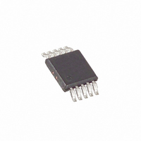
IC SWITCH DUAL SPDT 10UMAX

MAX4685EUB+

Manufacturer Part Number
MAX4685EUB+
Description
IC SWITCH DUAL SPDT 10UMAX
Manufacturer
Maxim Integrated Products
Datasheet

Specifications of MAX4685EUB+

Function
Switch
Circuit
2 x SPDT
On-state Resistance
800 mOhm
Voltage Supply Source
Single Supply
Voltage - Supply, Single/dual (±)
1.8 V ~ 5.5 V
Operating Temperature
-40°C ~ 85°C
Mounting Type
Surface Mount
Package / Case
10-MSOP, Micro10™, 10-uMAX, 10-uSOP
Number Of Switches
Dual
Switch Configuration
SPDT
On Resistance (max)
0.8 Ohms
On Time (max)
60 ns
Off Time (max)
40 ns
Off Isolation (typ)
- 64 dB
Supply Voltage (max)
5.5 V
Supply Voltage (min)
1.8 V
Maximum Power Dissipation
444 mW
Maximum Operating Temperature
+ 85 C
Mounting Style
SMD/SMT
Description/function
Analog Switch
Minimum Operating Temperature
- 40 C
Off State Leakage Current (max)
10 nA
Lead Free Status / RoHS Status
Lead free / RoHS Compliant
The MAX4684/MAX4685 low on-resistance (R
voltage, dual single-pole/double-throw (SPDT) analog
switches operate from a single +1.8V to +5.5V supply.
The MAX4684 features a 0.5Ω (max) R
switch and a 0.8Ω (max) R
+2.7V supply. The MAX4685 features a 0.8Ω max on-
resistance for both NO and NC switches at a +2.7V
supply.
Both parts feature break-before-make switching action
(2ns) with t
tal logic inputs are 1.8V logic-compatible with a +2.7V to
+3.3V supply.
The MAX4684/MAX4685 are packaged in the chipscale
package (UCSP)™, significantly reducing the required
PC board area. The chip occupies only a 2.0mm
1.50mm area. The 4
spaced with a 0.5mm bump pitch.
UCSP is a trademark of Maxim Integrated Products, Inc.
µMAX is a registered trademark of Maxim Integrated Products,
Inc.
For pricing, delivery, and ordering information, please contact Maxim Direct at 1-888-629-4642,
or visit Maxim’s website at www.maxim-ic.com.
________________________Applications
19-1977; Rev 4; 1/09
Continued at end of data sheet.
Speaker Headset Switching
MP3 Players
Power Routing
Battery-Operated Equipment
Relay Replacement
Audio and Video Signal Routing
Communications Circuits
PCMCIA Cards
Cellular Phones
Modems
ON
= 50ns and t
________________________________________________________________ Maxim Integrated Products
TOP VIEW
General Description
3 array of solder bumps are
OFF
COM1
ON
NC1
NO1
IN1
= 40ns at +3V. The digi-
C1
C2
C3
C4
for its NO switch at a
MAX4684/MAX4685
0.5 Ω Ω /0.8 Ω Ω Low-Voltage, Dual SPDT
Pin Configurations/Functional Diagrams/Truth Table
UCSP
GND
B1
B4
V+
ON
A1
A2
A3
A4
NC2
IN2
COM2
NO2
for its NC
ON
SWITCHES SHOWN FOR LOGIC "0" INPUT
), low-
IN_
0
1
MAX4684/MAX4685
Analog Switches in UCSP
NO_
OFF
ON
♦ 12-Bump, 0.5mm-Pitch UCSP
♦ NC Switch R
♦ NO Switch R
♦ R
♦ R
♦ +1.8V to +5.5V Single-Supply Operation
♦ Rail-to-Rail Signal Handling
♦ 1.8V Logic Compatibility
♦ Low Crosstalk: -68dB (100kHz)
♦ High Off-Isolation: -64dB (100kHz)
♦ THD: 0.03%
♦ 50nA (max) Supply Current
♦ Low Leakage Currents
+ Denotes a lead(Pb)-free/RoHS-compliant package.
Note: Requires special solder temperature profile described in
the Absolute Maximum Ratings section.
* UCSP reliability is integrally linked to the user’s assembly
methods, circuit board material, and environment. Refer to the
UCSP Reliability Notice in the UCSP Reliability section of this
data sheet for more information.
** EP = Exposed Pad
T = Tape and reel.
M A X4 6 8 4 E BC + T
M AX 4684E TB+ T
M AX 4684E U B+ T
M A X4 6 8 5 E BC + T
M AX 4685E TB+ T
M AX 4685E U B+ T
NC_
OFF
ON
ON
ON
0.5Ω max (+2.7V Supply) (MAX4684)
0.8Ω max (+2.7V Supply) (MAX4685)
0.8Ω max (+2.7V Supply)
0.06Ω (max)
0.15Ω (max)
1nA (max) at T
PART
Match Between Channels
Flatness Over Signal Range
COM1
NO1
NC1
IN1
V+
1
2
3
4
5
MAX4684/MAX4685
ON
ON
µMAX
-40°C to +85°C
-40°C to +85°C
-40°C to +85°C
-40°C to +85°C
-40°C to +85°C
-40°C to +85°C
TEMP RANGE
A
Ordering Information
= +25°C
10 NO2
9
8
7
6
COM2
IN2
NC2
GND
PIN /B U M P-
PACKAGE
12 UCSP*
10 TD FN - E P **
10 µMAX
12 UCSP*
10 TD FN - E P **
10 µMAX
Features
®
MARK
TOP
AAG
AAG
AAH
AAF
1

Related parts for MAX4685EUB+

MAX4685EUB+ Summary of contents

Page 1

... Power Routing Battery-Operated Equipment Relay Replacement Audio and Video Signal Routing Communications Circuits PCMCIA Cards Cellular Phones Modems UCSP is a trademark of Maxim Integrated Products, Inc. µMAX is a registered trademark of Maxim Integrated Products, Inc. Pin Configurations/Functional Diagrams/Truth Table TOP VIEW MAX4684/MAX4685 NC1 C1 ...

Page 2

Low-Voltage, Dual SPDT Analog Switches in UCSP ABSOLUTE MAXIMUM RATINGS (All Voltages Referenced to GND) V+, IN_......................................................................-0.3V to +6V COM_, NO_, NC_ (Note1) ........................... -0.3V to (V+ + 0.3V) Continuous Current NO_, NC_, COM_ ...

Page 3

Low-Voltage, Dual SPDT ELECTRICAL CHARACTERISTICS—+3V SUPPLY (continued) (V+ = +2.7V to +3.3V +1.4V (Notes 3, 9, 10) PARAMETER SYMBOL Turn-Off Time t OFF Break-Before-Make t BBM Delay Charge Injection ...

Page 4

Low-Voltage, Dual SPDT Analog Switches in UCSP (T = +25°C, unless otherwise noted.) A MAX4684 NC ON-RESISTANCE vs. COM VOLTAGE 1.8 1 +1.8V 1.4 1.2 1 +2. +5.0V ...

Page 5

Low-Voltage, Dual SPDT (T = +25°C, unless otherwise noted.) A SUPPLY CURRENT vs. SUPPLY VOLTAGE 100 (V) SUPPLY LOGIC THRESHOLD VOLTAGE vs. ...

Page 6

Low-Voltage, Dual SPDT Analog Switches in UCSP PIN NAME UCSP µMAX/TDFN NC_ A1, C1 IN_ A2, C2 COM_ A3, C3 NO_ A4 GND B1 EP — Detailed Description The MAX4684/MAX4685 are ...

Page 7

Low-Voltage, Dual SPDT UCSP Package Consideration For general UCSP package information and PC layout considerations, please refer to the Maxim Application Note (Wafer-Level Ultra-Chip-Board-Scale Package). UCSP Reliability The chip-scale package (UCSP) represents a unique ...

Page 8

Low-Voltage, Dual SPDT Analog Switches in UCSP MAX4684 MAX4685 R GEN NC_ OR NO_ V GEN GND IN_ Figure 4. Charge Injection +5V 10nF IN_ MAX4684 NC_ MAX4685 50Ω GND ...

Page 9

Low-Voltage, Dual SPDT For the latest package outline information and land patterns www.maxim-ic.com/packages. PACKAGE TYPE 12 UCSP 10 TDFN-EP 10 µMAX _______________________________________________________________________________________ Analog Switches in UCSP Package Information PACKAGE CODE B12-4 T1033-1 ...

Page 10

... Maxim cannot assume responsibility for use of any circuitry other than circuitry entirely embodied in a Maxim product. No circuit patent licenses are implied. Maxim reserves the right to change the circuitry and specifications without notice at any time. 10 ____________________Maxim Integrated Products, 120 San Gabriel Drive, Sunnyvale, CA 94086 408-737-7600 © 2009 Maxim Integrated Products DESCRIPTION is a registered trademark of Maxim Integrated Products ...

Related keywords