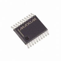
MAX333ACUP+ Maxim Integrated Products, MAX333ACUP+ Datasheet - Page 5

MAX333ACUP+
Manufacturer Part Number
MAX333ACUP+
Description
IC SWITCH QUAD SPDT 20TSSOP
Manufacturer
Maxim Integrated Products
Datasheet
1.MAX333ACPP.pdf
(8 pages)
Specifications of MAX333ACUP+
Function
Switch
Circuit
4 x SPDT
On-state Resistance
35 Ohm
Voltage Supply Source
Single, Dual Supply
Voltage - Supply, Single/dual (±)
10 V ~ 30 V, ±4.5 V ~ 20 V
Current - Supply
1µA
Operating Temperature
0°C ~ 70°C
Mounting Type
Surface Mount
Package / Case
20-TSSOP
Number Of Switches
Quad
Switch Configuration
SPDT
On Resistance (max)
45 Ohms
On Time (max)
175 ns
Off Time (max)
145 ns
Off Isolation (typ)
72 dB
Supply Voltage (max)
+/- 20 V
Supply Voltage (min)
+/- 4.5 V
Supply Current
0.05 mA
Maximum Power Dissipation
559 mW
Maximum Operating Temperature
+ 70 C
Mounting Style
SMD/SMT
Description/function
Analog Switch
Input Level
CMOS, TTL
Minimum Operating Temperature
0 C
Off State Leakage Current (max)
1 nA
Lead Free Status / RoHS Status
Lead free / RoHS Compliant
The main limitation of supply voltages other than ±15V is
a reduction in the analog signal range. The MAX333A
operates with ±5V to ±20V bipolar supplies. The
Typical Operating Characteristics and graphs show typ-
ical on resistance for ±15V, ±10V, ±5 supplies.
Switching times increase by a factor of two or more for
±5V operation. The MAX333A can operate from +10V
to +24V unipolar supplies. It can be powered from a
single +10V to +24V supply, as well as from unbalanced
supplies such as +24V and -5V. Connect V- to 0V when
operating with a single supply.
_____________________Pin Description
______________________________________________Test Circuits/Timing Diagrams
Figure 2. Switching-Time Test Circuit
__________Applications Information
1, 10, 11, 20
2, 9, 12, 19
3, 8, 13, 18
4, 7, 14, 17
PIN
15
16
5
6
V
Precision, Quad, SPDT, CMOS Analog Switch
COM
V
IN
+10V
-10V
3V
0V
0V
Operation with Supply Voltages
t
OFF
COM1-COM4
_______________________________________________________________________________________
NO1-NO4
NC1-NC4
IN1-IN4
NAME
GND
N.C.
V+
V-
50%
t
t
50%
ON
t
t
OPEN
R
F
50%
< 20ns
< 20ns
t
OFF
Logic-Level Inputs
Normally Open Switches
Common Switch Poles
Normally Closed Switches
Negative Power Supply
Ground
Not Internally Connected
Positive Power Supply
Other than ±15V
FUNCTION
50%
t
ON
t
OPEN
50%
50%
o
Proper power-supply sequencing is recommended for
all CMOS devices. It is important not to exceed the
absolute maximum ratings because stresses beyond
the listed ratings may cause permanent damage to the
devices. Always sequence V+ on first, followed by VL,
V-, and logic inputs. If power-supply sequencing is not
possible, add two small signal diodes in series with the
supply pins (Figure 1). Adding the diodes reduces the
analog signal range to 1V below V+ and 1V below V-,
but low switch resistance and low leakage characteris-
tics are unaffected.
Figure 1. Overvoltage Protection Using Blocking Diodes
LOGIC
INPUT
+10V
-10V
IN_
V
g
(REPEAT TEST FOR IN2, IN3, AND IN4.)
+15V
V+
COM_
NO_
NC_
GND
Overvoltage Protection
V+
V-
COM_
-15V
V-
SWITCH OUTPUT
( OR NC_)
NO_
300
5


