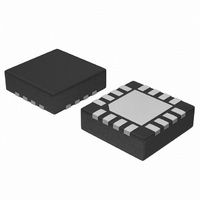
NBSG72AMNG ON Semiconductor, NBSG72AMNG Datasheet

NBSG72AMNG
Specifications of NBSG72AMNG
Available stocks
Related parts for NBSG72AMNG
NBSG72AMNG Summary of contents
Page 1
NBSG72A 2.5V/3.3V SiGe Differential Crosspoint Switch with Output Level Select The NBSG72A is a high−bandwidth fully differential crosspoint switch with Output Level Select (OLS) capabilities. This is a part of the GigaComm™ family of high ...
Page 2
Table 1. PIN DESCRIPTION Pin No. Name I/O 1 VTD0 2 D0 LVDS, CML, ECL, LVTTL, LVCMOS Input 3 D0 LVDS, CML, ECL, LVTTL, LVCMOS Input 4 SELA LVECL, LVCMOS Input Á Á Á Á Á Á ...
Page 3
VTD0 VTD1 2 SELA SELB 75 kW OLS Figure 2. Logic/Block Diagram Table 3. OUTPUT LEVEL SELECT (OLS) OLS ...
Page 4
Table 5. ATTRIBUTES Internal Input Pulldown Resistor (SELA, SELB) ESD Protection Moisture Sensitivity (Note 1) Flammability Rating Transistor Count Meets or exceeds JEDEC Spec EIA/JESD78 IC Latchup Test 1. For additional information, see Application Note AND8003/D. Table 6. MAXIMUM RATINGS ...
Page 5
Table 7. DC CHARACTERISTICS, INPUT WITH PECL OUTPUT Symbol Characteristic I Negative Power Supply Current EE V Output HIGH Voltage (Note Output LOW Voltage (Note 4) OL (OLS = V (OLS = V − 0.8 V, OLS ...
Page 6
Table 8. DC CHARACTERISTICS, INPUT WITH PECL OUTPUT Symbol Characteristic I Negative Power Supply Current EE V Output HIGH Voltage (Note Output LOW Voltage (Note 9) OL (OLS = V (OLS = V − 0.8 V, OLS ...
Page 7
Table 9. DC CHARACTERISTICS, NECL INPUT WITH NECL OUTPUT Symbol Characteristic I Negative Power Supply Current EE V Output HIGH Voltage (Note 14 Output LOW Voltage (Note 14) OL −3.465 −3 (OLS ...
Page 8
Table 10. AC CHARACTERISTICS Symbol Characteristic V Output Voltage Amplitude OUTPP (Note 18) t Propagation Delay to Output Differential PLH D0, D1 → Q0, Q1 SELA, SELB → Q0 Propagation Delay to Output Differential PHL D0, D1 → ...
Page 9
OLS = V 800 700 OLS = V 600 500 *OLS = V 400 300 OLS = V 200 100 0 1 Figure 3. Output Voltage Amplitude (V Input Clock Frequency (f *When an output level of 400 mV ...
Page 10
D0 Q0 Non−Driven Signal Path Input Input Signal NBSG72A D1 Q1 SELA SELB Logic Logic Low Low Figure 6. Channel−to−Channel Crosstalk Isolation at Ambient Temperature ( and Q1 Signal Path Selected; SelA = Low, ...
Page 11
Figure 8. Eye Diagram at 3.2 Gb/s (V − 3.3 V, OLS = FLOAT @ 255C with input pattern Figure 9. Eye Diagram at 7 Gb/s/s (V − 3.3 V, OLS = ...
Page 12
V − 800 V − 700 CC 600 400 V − 250 V − 550 CC CC 200 − 400 V − 800 OLS (mV) Figure 11. OLS Operating Area D ...
Page 13
... ORDERING INFORMATION Device NBSG72AMN NBSG72AMNG NBSG72AMNR2 NBSG72AMNR2G Board NBSG72AMNEVB †For information on tape and reel specifications, including part orientation and tape sizes, please refer to our Tape and Reel Packaging Specifications Brochure, BRD8011/D. Resource Reference of Application Notes AN1405/D AN1406/D AN1503/D AN1504/D AN1568/D AN1672/D AND8001/D − ...
Page 14
... Opportunity/Affirmative Action Employer. This literature is subject to all applicable copyright laws and is not for resale in any manner. PUBLICATION ORDERING INFORMATION LITERATURE FULFILLMENT: Literature Distribution Center for ON Semiconductor P.O. Box 5163, Denver, Colorado 80217 USA Phone: 303−675−2175 or 800−344−3860 Toll Free USA/Canada Fax: 303− ...


