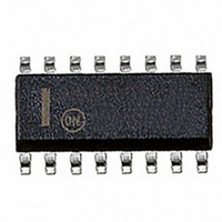
MC14053BDR2G ON Semiconductor, MC14053BDR2G Datasheet

IC MUX/DEMUX TRIPLE 2X1 16SOIC

MC14053BDR2G

Manufacturer Part Number
MC14053BDR2G
Description
IC MUX/DEMUX TRIPLE 2X1 16SOIC
Manufacturer
ON Semiconductor
Series
4000Br
Type
Analog Multiplexerr
Datasheets

Specifications of MC14053BDR2G

Function
Multiplexer/Demultiplexer
Circuit
3 x 2:1
On-state Resistance
280 Ohm
Voltage Supply Source
Dual Supply
Voltage - Supply, Single/dual (±)
±3 V ~ 18 V
Current - Supply
0.36µA
Operating Temperature
-55°C ~ 125°C
Mounting Type
Surface Mount
Package / Case
16-SOIC (0.154", 3.90mm Width)
On Resistance (max)
1050 Ohms
Propagation Delay Time
65 ns
On Time (max)
550 ns
Off Time (max)
550 ns
Supply Voltage (max)
18 V
Supply Voltage (min)
3 V
Maximum Power Dissipation
500 mW
Maximum Operating Temperature
+ 125 C
Minimum Operating Temperature
- 55 C
Mounting Style
SMD/SMT
Number Of Switches
Triple
Current, Supply
600 μA
Function Type
2-Channels
Logic Function
Multiplexer/Demultiplexer
Logic Type
CMOS
Package Type
SOIC-16
Special Features
Digitally-Controlled Analog Switch, Triple SPDT
Temperature, Operating, Range
-55 to +125 °C
Voltage, Supply
3 to 18 VDC
Multiplexer Configuration
Triple 2:1
Number Of Inputs
6
Number Of Outputs
3
Number Of Channels
3
Analog Switch On Resistance
1050@5VOhm
Analog Switch Turn On Time
550ns
Analog Switch Turn Off Time
550ns
Power Supply Requirement
Single
Single Supply Voltage (min)
3V
Single Supply Voltage (typ)
5/9/12/15V
Single Supply Voltage (max)
18V
Dual Supply Voltage (min)
Not RequiredV
Dual Supply Voltage (typ)
Not RequiredV
Dual Supply Voltage (max)
Not RequiredV
Power Dissipation
500mW
Mounting
Surface Mount
Pin Count
16
Operating Temp Range
-55C to 125C
Operating Temperature Classification
Military
Lead Free Status / RoHS Status
Lead free / RoHS Compliant
Other names
MC14053BDR2GOSTR

Available stocks

Company
Part Number
Manufacturer
Quantity
Price
Part Number:
MC14053BDR2G
Manufacturer:
LT
Quantity:
6 700
Part Number:
MC14053BDR2G
Manufacturer:
ON Semiconductor
Quantity:
1 843
Part Number:
MC14053BDR2G
Manufacturer:
ON41
Quantity:
2 500
Part Number:
MC14053BDR2G
Manufacturer:
ON/安森美
Quantity:
20 000
Part Number:
MC14053BDR2G
0
Company:
Part Number:
MC14053BDR2G
Quantity:
7 500
MC14051B, MC14052B,
MC14053B
Analog
Multiplexers/Demultiplexers
are digitally−controlled analog switches. The MC14051B effectively
implements an SP8T solid state switch, the MC14052B a DP4T, and
the MC14053B a Triple SPDT. All three devices feature low ON
impedance and very low OFF leakage current. Control of analog
signals up to the complete supply voltage range can be achieved.
Features
Stresses exceeding Maximum Ratings may damage the device. Maximum
Ratings are stress ratings only. Functional operation above the Recommended
Operating Conditions is not implied. Extended exposure to stresses above the
Recommended Operating Conditions may affect device reliability.
1. Temperature Derating: Plastic “P and D/DW” Packages: – 7.0 mW/_C From
static voltages or electric fields. However, precautions must be taken to avoid
applications of any voltage higher than maximum rated voltages to this
high−impedance circuit. For proper operation, V
the range V
V
*For additional information on our Pb−Free strategy and soldering details, please
MAXIMUM RATINGS
© Semiconductor Components Industries, LLC, 2006
Symbol
download the ON Semiconductor Soldering and Mounting Techniques
Reference Manual, SOLDERRM/D.
SS
The MC14051B, MC14052B, and MC14053B analog multiplexers
This device contains protection circuitry to guard against damage due to high
Unused inputs must always be tied to an appropriate logic voltage level (e.g., either
Note: V
CMOS Devices
Triple Diode Protection on Control Inputs
Switch Function is Break Before Make
Supply Voltage Range = 3.0 Vdc to 18 Vdc
Analog Voltage Range (V
Linearized Transfer Characteristics
Low−noise − 12 nV/√Cycle, f ≥ 1.0 kHz Typical
Pin−for−Pin Replacement for CD4051, CD4052, and CD4053
For 4PDT Switch, See MC14551B
For Lower R
Pb−Free Packages are Available*
V
V
V
I
T
65_C To 125_C
P
SW
T
T
, V
I
DD
out
stg
in
in
A
D
L
,
EE
or V
SS
DC Supply Voltage Range
(Referenced to V
Input or Output Voltage Range
(DC or Transient) (Referenced to V
Control Inputs and V
Input Current (DC or Transient)
per Control Pin
Switch Through Current
Power Dissipation per Package (Note 1)
Ambient Temperature Range
Storage Temperature Range
Lead Temperature (8−Second Soldering)
EE
DD
v (V
must be v V
). Unused outputs must be left open.
ON
in
, Use the HC4051, HC4052, or HC4053 High−Speed
or V
(Voltages Referenced to V
out
Parameter
) v V
EE
SS
, V
EE
DD
DD
SS
for Switch I/O)
.
− V
≥ V
EE
EE
)
) = 3.0 to 18 V
in
SS
and V
for
SS
out
−0.5 to V
)
should be constrained to
−0.5 to +18.0
−55 to +125
−65 to +150
Value
+10
± 25
500
260
DD
+ 0.5
1
Unit
mW
mA
mA
°C
°C
°C
V
V
See detailed ordering and shipping information in the package
dimensions section on page 9 of this data sheet.
1
(Note: Microdot may be in either location)
1
1
1
x
A
WL, L
Y
WW, W
G or G
ORDERING INFORMATION
CASE 751B
CASE 948F
SOEIAJ−16
DT SUFFIX
TSSOP−16
CASE 648
CASE 966
P SUFFIX
D SUFFIX
F SUFFIX
SOIC−16
PDIP−16
= 1, 2, or 3
= Assembly Location
= Wafer Lot
= Year
= Work Week
= Pb−Free Package
Publication Order Number:
16
16
1
16
1
1
16
1
DIAGRAMS
MC1405xBCP
MARKING
AWLYYWWG
MC1405xB
AWLYWW
1405xBG
ALYWG
ALYWG
MC14051B/D
05xB
14
G
Related parts for MC14053BDR2G

MC14053BDR2G Summary of contents

Page 1

... Unused inputs must always be tied to an appropriate logic voltage level (e.g., either Unused outputs must be left open *For additional information on our Pb−Free strategy and soldering details, please download the ON Semiconductor Soldering and Mounting Techniques Reference Manual, SOLDERRM/D. © Semiconductor Components Industries, LLC, 2006 ) = 3 Value Unit −0.5 to +18.0 ...

Page 2

ELECTRICAL CHARACTERISTICS Î Î Î Î Î ...

Page 3

ELECTRICAL CHARACTERISTICS Î Î Î Î Î ...

Page 4

... MC14052BF MC14052BFG MC14052BFEL MC14052BFELG MC14053BCP MC14053BCPG MC14053BD MC14053BDG MC14053BDR2 MC14053BDR2G MC14053BDTR2 MC14053BDTR2G MC14053BF MC14053BFG MC14053BFEL MC14053BFELG †For information on tape and reel specifications, including part orientation and tape sizes, please refer to our Tape and Reel Packaging Specifications Brochure, BRD8011/D. *This package is inherently Pb−Free. ...

Page 5

MC14051B, MC14052B, MC14053B −A− 0.25 (0.010) M −A− −B− −T− SEATING PLANE 0.25 (0.010 ...

Related keywords