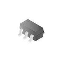
DG9421DV-T1-E3 Vishay, DG9421DV-T1-E3 Datasheet

DG9421DV-T1-E3
Specifications of DG9421DV-T1-E3
Available stocks
Related parts for DG9421DV-T1-E3
DG9421DV-T1-E3 Summary of contents
Page 1
... Switches Shown for Logic "0" Input ORDERING INFORMATION IN NO Temp. Range GND - 40 ° °C DG9421, DG9422 Vishay Siliconix : 2.0 Ω DS(on OFF in small TSOP package ON DG9421 DG9422 OFF Package Part Number DG9421DV-T1 DG9421DV-T1-E3 6/Pin TSOP DG9422DV-T1 DG9422DV-T1-E3 www.vishay.com Pb-free Available RoHS* COMPLIANT OFF ON 1 ...
Page 2
... DG9421, DG9422 Vishay Siliconix ABSOLUTE MAXIMUM RATINGS Parameter GND Continuous Current (Any Terminal) Peak Current (Pulsed Duty Cycle) Storage Temperature b Power Dissipation (Packages) Notes: a. Signals exceeding will be clamped by internal diodes. Limit forward diode current to maximum current ratings All leads welded or soldered to PC board. ...
Page 3
... V = ± 4 Under Test = 0 Under Test = 2 300 Ω pF ± 3 See Figure Ω Ω MHz MHz DG9421, DG9422 Vishay Siliconix Limits - 40 ° ° Temp. Min. Typ. Max. Unit Full - Room 2.2 3.2 Ω Full 3.6 Room - 1 1 Full - 10 10 Room - Full - 10 10 ...
Page 4
... DG9421, DG9422 Vishay Siliconix a SPECIFICATIONS Single Supply 5 V Parameter Symbol Analog Switch e V Analog Signal Range ANALOG Drain-Source R DS(on) On-Resistance Dynamic Characteristics e t Turn-On Time Turn-Off Time OFF e Q Charge Injection Power Supplies e I+ Positive Supply Current e I- Negative Supply Current ...
Page 5
... 3 Under Test = 0 Under Test = 2 300 Ω pF 1 See Figure Ω Ω MHz MHz DG9421, DG9422 Vishay Siliconix Limits - 40 ° ° Temp Min. Typ. Max. Unit Full Room 7.3 8.8 Ω Full 10.1 Room - 1 1 Full - 10 10 Room - Full - 10 10 Room - 1 1 Full ...
Page 6
... DG9421, DG9422 Vishay Siliconix TYPICAL CHARACTERISTICS 25 °C, unless otherwise noted ° 3 5 Analog Voltage ( vs. V and Supply Voltage ON COM 8 V± = ± ° ° ° Drain V oltage (V) R vs. Analog Voltage and Temperature 100 µ 10 µ 1 µ 100 100 1K 10K Input Switching Frequences (Hz) Supply Current vs ...
Page 7
... NO NC Leakage vs. Analog Voltage 10 Loss Ω OIRR - 100K 1M 10M Frequency ( Insertion Loss, Off Isolation vs. Frequency Document Number: 70679 S-82265-Rev. F, 29-Sep- 100 100 100M 1G DG9421, DG9422 Vishay Siliconix 100 NC on Analog Voltage (V) COM NO NC Leakage vs. Analog Voltage 120 100 OFF t 40 OFF ...
Page 8
... DG9421, DG9422 Vishay Siliconix TYPICAL CHARACTERISTICS 25 °C, unless otherwise noted 300 250 200 150 100 100 - 150 - 200 - 250 - 300 Analog Voltage (V) COM Charge Injection vs. Analog Voltage SCHEMATIC DIAGRAM Typical Channel GND V- TEST CIRCUITS 300 V- GND V- C (includes fixture and stray capacitance) ...
Page 9
... Bypass Figure 5. Off Isolation Vishay Siliconix maintains worldwide manufacturing capability. Products may be manufactured at one of several qualified locations. Reliability data for Silicon Technology and Package Reliability represent a composite of all qualified locations. For related documents such as package/tape drawings, part marking, and reliability data, see http://www.vishay.com/ppg?70679. ...
Page 10
... Vishay product could result in personal injury or death. Customers using or selling Vishay products not expressly indicated for use in such applications their own risk and agree to fully indemnify and hold Vishay and its distributors harmless from and against any and all claims, liabilities, expenses and damages arising or resulting in connection with such use or sale, including attorneys fees, even if such claim alleges that Vishay or its distributor was negligent regarding the design or manufacture of the part ...


