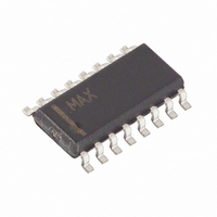
MAX4638ESE+ Maxim Integrated Products, MAX4638ESE+ Datasheet - Page 6

MAX4638ESE+
Manufacturer Part Number
MAX4638ESE+
Description
IC MULTIPLEXER 8X1 16SOIC
Manufacturer
Maxim Integrated Products
Type
Analog Multiplexerr
Datasheet
1.MAX4639ESE.pdf
(16 pages)
Specifications of MAX4638ESE+
Function
Multiplexer
Circuit
1 x 8:1
On-state Resistance
3.5 Ohm
Voltage Supply Source
Single, Dual Supply
Voltage - Supply, Single/dual (±)
1.8 V ~ 5.5 V, ±2.5 V
Current - Supply
1µA
Operating Temperature
-40°C ~ 85°C
Mounting Type
Surface Mount
Package / Case
16-SOIC (0.154", 3.90mm Width)
Number Of Channels
1 Channel
On Resistance (max)
6 Ohms at 3.3 V
Propagation Delay Time
18 ns at 5 V, 20 ns at 3.3 V, 20 ns at +/- 2.5 V
On Time (max)
20 ns at 3.3 V
Off Time (max)
9 ns at 3.3 V
Supply Voltage (max)
5.5 V
Supply Voltage (min)
1.8 V
Maximum Power Dissipation
696 mW
Maximum Operating Temperature
+ 85 C
Minimum Operating Temperature
- 40 C
Mounting Style
SMD/SMT
Switch Current (typ)
0.000001 mA at 5.5 V
Lead Free Status / RoHS Status
Lead free / RoHS Compliant
3.5Ω, Single 8:1 and Dual 4:1,
Low-Voltage Analog Multiplexers
ELECTRICAL CHARACTERISTICS—±2.5V Dual Supplies (continued)
(V+ = +2.5 ±10%, V- = -2.5V ±10%, V
V± = ±2.5V and T
Note 2: The algebraic convention, where the most negative value is a minimum and the most positive value a maximum, is used in
Note 3: ∆R
Note 4: Flatness is defined as the difference between the maximum and minimum value of on-resistance as measured over the
Note 5: Guaranteed by design.
Note 6: Off-Isolation = 20log
Note 7: Between any two switches.
Note 8: ∆R
Note 9: Parts are tested at +85°C and guaranteed by design over the entire temperature range.
6
On-Resistance Flatness
(Note 4)
NO_ Off-Leakage
Current (Note 5)
COM_ Off-Leakage
Current (Note 5)
COM_ On-Leakage
Current (Note 5)
DIGITAL I/O
Input Logic High
Input Logic Low
Input Leakage Current
Digital Input Capacitance
DYNAMIC
Transition Time (Note 5)
Enable Turn-On Time
(Note 5)
Enable Turn-Off Time
(Note 5)
Break-Before-Make (Note 5)
______________________________________________________________________________________
this data sheet.
specified analog signal ranges.
PARAMETER
ON
ON
= R
matching specifications for thin QFN packaged parts are guaranteed by design.
A
ON(MAX)
= +25°C.)
- R
10
ON(MIN)
(V
COM_
I
I
COM_ (OFF)
R
I
SYMBOL
COM_ (ON)
NO_ (OFF)
t
t
FLAT(ON)
t
OFF(EN)
.
ON(EN)
I
TRANS
t
IH
C
BBM
V
V
IH
/ V
IH
, I
IL
IN
IL
NO_
= +2.0V, V
), V
I
0; V + = + 2.25V ; V - = - 2.25V
V + = + 2.75V; V - = -2.75V ;
V
V
V + = + 2.75V; V - = -2.75;
V
V
V + = + 2.5V ; V - = - 2.5;
V
V
fl oati ng
V
V
R
V
R
V
R
V
R
C OM_
COM_
NO_
C OM_
N O_
C OM _
NO_
IN_
NO_
N O_
N O_
N O_
L
L
L
L
COM_
= 100 , Figure 2
= 100 , Figure 4
= 100 , Figure 4
= 100 , Figure 3
= 0 or V+
= +2.5V, + 1V
= + 1.2V , C
= +1.2V, C
= + 1.2V , C
= +2.5V, +1V
= + 1V , + 2.5V , or
= +1.2V, C
= 10m A; V
IL
= +1V , + 2.5V ;
= + 1V , + 2.5V ;
= +1V, +2.5V;
= output, V
= +0.4V, T
L
N O_
L
L
CONDITIONS
L
= 35p F,
= 35p F,
= 35p F,
= 35pF,
NO_
= 1.5V ,
A
= T
= input to off switch.
MIN
T
T
T
T
T
T
T
T
T
T
T
T
T
T
T
T
A
A
A
A
A
A
A
A
A
A
A
A
A
A
A
A
to T
= +25°C
= +25°C
= +25°C
= +25°C
= +25°C
= +25°C
= T
= +25°C
= T
= +25°C
= T
= T
= T
= T
= T
= T
MAX
MIN
MIN
MIN
MIN
MIN
MIN
MIN
MIN
, unless otherwise noted. Typical values are at
to T
to T
to T
to T
to T
to T
to T
to T
MAX
MAX
MAX
MAX
MAX
MAX
MAX
MAX
-0.25
-0.35
-0.25
-0.35
-0.25
-0.35
MIN
-0.1
2.0
1
( N o t e 2 )
0.005
TYP
0.75
0.01
0.01
0.01
16
14
2
5
8
MAX
0.25
0.35
0.25
0.35
0.25
0.35
1.2
0.4
0.1
20
24
18
20
1
7
8
UNITS
nA
nA
nA
µA
pF
ns
ns
ns
ns
V
V


