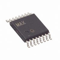
DG411FEUE+ Maxim Integrated Products, DG411FEUE+ Datasheet - Page 9

DG411FEUE+
Manufacturer Part Number
DG411FEUE+
Description
IC SWITCH QUAD SPST 16TSSOP
Manufacturer
Maxim Integrated Products
Type
Analog Switchr
Datasheet
1.DG411FEUE.pdf
(16 pages)
Specifications of DG411FEUE+
Function
Switch
Circuit
4 x SPST - NC
On-state Resistance
45 Ohm
Voltage Supply Source
Single, Dual Supply
Voltage - Supply, Single/dual (±)
10 V ~ 30 V, ±4.5 V ~ 20 V
Operating Temperature
0°C ~ 70°C
Mounting Type
Surface Mount
Package / Case
16-TSSOP
Package
16TSSOP
Maximum On Resistance
85@12V Ohm
Maximum Low Level Output Current
30 mA
Maximum Turn-off Time
145@±15V ns
Maximum Turn-on Time
250@12V ns
Switch Architecture
SPST
Power Supply Type
Single|Dual
Lead Free Status / RoHS Status
Lead free / RoHS Compliant
The DG411F/DG412F/DG413F are fault-protected
CMOS analog switches with unique operation and
construction. These switches differ considerably from
traditional fault-protection switches, with several advan-
tages. First, they are constructed with two parallel
FETs, allowing very low on-resistance when the switch
is on. Second, they allow signals on the NO_ or NC_
pins that are within, or slightly beyond, the supply rails
to be passed through the switch to the COM_ terminal
(or vice versa), allowing true rail-to-rail signal operation.
Third, the DG411F/DG412F/DG413F have the same
fault-protection performance on any of the NO_, NC_,
or COM_ switch inputs. Operation is identical for both
fault polarities. The fault protection extends to ±36V
from GND with ±15V supplies.
During a fault condition, the particular overvoltage input
(COM_, NO_, NC_) pin becomes high impedance
regardless of the switch state or load resistance. When
power is removed, the fault protection is still in effect. In
this case, the COM_, NO_, or NC_ terminals are a virtu-
al open circuit. The fault can be up to ±40V with power
off. The switches turn off when V+ is not powered,
regardless of V-.
These switches have identical pinouts to common non-
fault-protected CMOS switches. They allow for carefree
2, 15, 10, 7
3, 14, 11, 6
1, 16, 9, 8
DG411F
12
13
—
—
—
4
5
2, 15, 10, 7
3, 14, 11, 6
1, 16, 9, 8
DG412F
PIN
_______________________________________________________________________________________
12
13
—
—
—
4
5
Detailed Description
2, 15, 10, 7
1, 16, 9, 8
DG413F
14, 11
3, 6
Quad, Rail-to-Rail, Fault-Protected,
12
13
—
—
4
5
Pin Compatibility
COM1, COM2, COM3,
NO1, NO2, NO3, NO4
NC1, NC2, NC3, NC4
IN1, IN2, IN3, IN4
NO1, NO4
NC2, NC3
NAME
COM4
GND
N.C.
V+
V-
direct replacement in existing printed circuit boards
since the NO_, NC_, and COM_ pins of each switch are
fault protected.
Internal construction is shown in
log signal paths shown in bold. A single NO switch is
shown. The NC configuration is identical except the
logic-level translator becomes an inverter. The analog
switch is formed by the parallel combination of N-chan-
nel FET (N1) and P-channel FET (P1), which are driven
on and off simultaneously according to the input fault
condition and the logic-level state.
Two comparators continuously compare the voltage on
the COM_, NO_, and NC_ pins with V+ and V-. When
the signal on COM_, NO_, or NC_ is between V+ and
V-, the switch acts normally, with FETs N1 and P1 turn-
ing on and off in response to IN_ signals. The parallel
combination of N1 and P1 forms a low-value resistor
between NO_ (or NC_) and COM_ so that signals pass
equally well in either direction.
When the signal on NO_ (or NC_) and COM_ exceeds
V+ by about 50mV, the high-fault comparator output is
high, turning off FETs N1 and P1. This makes the NO_
(or NC_) and COM_ pins high impedance regardless of
SPST Analog Switches
Logic Control Digital Inputs
Analog Switch Common Terminals
Analog Switch Normally Closed Terminals
Analog Switch Normally Open Terminals
Analog Switch Normally Open Terminals
Analog Switch Normally Closed Terminals
Negative-Supply Voltage Input. Connect to GND for single-
supply operation. Bypass with a 0.1µF capacitor to GND.
Ground. Connect to digital ground.
No Connection. Not internally connected.
Positive-Supply Voltage Input. Bypass with a 0.1µF capacitor
to GND.
FUNCTION
Positive Fault Condition
Internal Construction
Pin Description
Normal Operation
Figure 1, with the ana-
9


