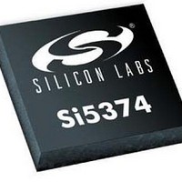
SI5374B-A-GL Silicon Laboratories Inc, SI5374B-A-GL Datasheet - Page 21

SI5374B-A-GL
Manufacturer Part Number
SI5374B-A-GL
Description
Clock Synthesizer / Jitter Cleaner QUAD DSPLL JITT ATT CLK LO LP BW 8IN/OUT
Manufacturer
Silicon Laboratories Inc
Datasheet
1.SI5374B-A-GL.pdf
(64 pages)
Specifications of SI5374B-A-GL
Package / Case
PBGA-80
Input Level
LVCMOS
Max Input Freq
525 Hz
Max Output Freq
808 MHz
Maximum Operating Temperature
+ 85 C
Minimum Operating Temperature
- 40 C
Number Of Outputs
8
Output Level
LVCMOS
Supply Current
1100 mA
Supply Voltage (max)
2.8 V
Supply Voltage (min)
- 0.5 V
Lead Free Status / Rohs Status
Compliant
Available stocks
Company
Part Number
Manufacturer
Quantity
Price
Company:
Part Number:
SI5374B-A-GL
Manufacturer:
SILICON
Quantity:
1 001
Company:
Part Number:
SI5374B-A-GL
Manufacturer:
Silicon Laboratories Inc
Quantity:
10 000
Reset value = 0000 0101
Register 3.
Name
Type
7:6
3:0
Bit
Bit
5
4
CKSEL_REG
SQ_ICAL
Reserved
DHOLD
CKSEL_REG[1:0]
Name
D7
[1:0]
R/W
CKSEL_REG.
If the device is operating in register-based manual clock selection mode
(AUTOSEL_REG = 00), and CKSEL_PIN = 0, then these bits select which input clock
will be the active input clock. If CKSEL_PIN = 1 and AUTOSEL_REG = 00, the CS_CA
input pin continues to control clock selection and
00: CKIN_1 selected.
01: CKIN_2 selected.
10: Reserved
11: Reserved
DHOLD.
Forces the device into digital hold. This bit overrides all other manual and automatic clock
selection controls.
0: Normal operation.
1: Force digital hold mode. Overrides all other settings and ignores the quality of the input
clocks.
SQ_ICAL.
This bit determines if the output clocks will remain enabled or be squelched (disabled)
during an internal calibration. See Table 8 on page 52.
0: Output clocks enabled during ICAL.
1: Output clocks disabled during ICAL.
D6
DHOLD
R/W
D5
Preliminary Rev. 0.4
SQ_ICAL
R/W
D4
Function
D3
R
CKSEL_
D2
R
REG is of no consequence.
D1
R
Si5374
D0
R
21


