ADG3249BRJ-REEL Analog Devices Inc, ADG3249BRJ-REEL Datasheet
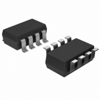
IC MUX/DEMUX 2X1 SOT23-8

ADG3249BRJ-REEL

Manufacturer Part Number
ADG3249BRJ-REEL
Description
IC MUX/DEMUX 2X1 SOT23-8
Manufacturer
Analog Devices Inc
Datasheet

Specifications of ADG3249BRJ-REEL

Rohs Status
RoHS non-compliant
Function
Multiplexer/Demultiplexer
Circuit
1 x 2:1
On-state Resistance
8 Ohm
Voltage Supply Source
Single Supply
Voltage - Supply, Single/dual (±)
2.3 V ~ 3.6 V
Current - Supply
0.01µA
Operating Temperature
-40°C ~ 85°C
Mounting Type
Surface Mount
Package / Case
SOT-23-8

Available stocks

Company
Part Number
Manufacturer
Quantity
Price
Part Number:
ADG3249BRJ-REEL7
Manufacturer:
ADI/亚德诺
Quantity:
20 000
GENERAL DESCRIPTION
The ADG3249 is a 2.5 V or 3.3 V, high performance 2:1 multi-
plexer/demultiplexer bus switch. It is designed on a low voltage
CMOS process, which provides low power dissipation yet gives
high switching speed and very low on resistance. This allows the
input to be connected to the output without additional propaga-
tion delay or generating additional ground bounce noise.
Each switch of the ADG3249 conducts equally well in both direc-
tions when on. The ADG3249 exhibits break-before-make
switching action, preventing momentary shorting when switch-
ing channels.
This device is ideal for applications requiring level translation.
When operated from a 3.3 V supply, level translation from
3.3 V inputs to 2.5 V outputs is allowed. Similarly, if the device
is operated from 2.5 V supply and 2.5 V inputs are applied, the
device will translate the outputs to 1.8 V. In addition, a level
translating pin (SEL) is included. When SEL is low, V
reduced internally, allowing for level translating between 3.3 V
inputs and 1.8 V outputs.
The ADG3249 is available in a tiny 8-lead SOT-23 package.
REV. 0
Information furnished by Analog Devices is believed to be accurate and
reliable. However, no responsibility is assumed by Analog Devices for its
use, nor for any infringements of patents or other rights of third parties that
may result from its use. No license is granted by implication or otherwise
under any patent or patent rights of Analog Devices. Trademarks and
registered trademarks are the property of their respective companies.
FEATURES
225 ps Propagation Delay through the Switch
4.5
Data Rate 1.244 Gbps
2.5 V/3.3 V Supply Operation
Selectable Level Shifting/Translation
Level Translation
Small Signal Bandwidth 610 MHz
8-Lead SOT-23 Package
APPLICATIONS
3.3 V to 1.8 V Voltage Translation
3.3 V to 2.5 V Voltage Translation
2.5 V to 1.8 V Voltage Translation
Docking Stations
Memory Switching
Analog Switch Applications
3.3 V to 2.5 V
3.3 V to 1.8 V
2.5 V to 1.8 V
Switch Connection between Ports
CC
is
PRODUCT HIGHLIGHTS
1. 3.3 V or 2.5 V supply operation.
2. Extremely low propagation delay through switch.
3. 4.5 Ω switches connect inputs to outputs.
4. Tiny SOT-23 package.
One Technology Way, P.O. Box 9106, Norwood, MA 02062-9106, U.S.A.
Tel: 781/329-4700
Fax: 781/326-8703
2.5 V/3.3 V, 2:1 Multiplexer/
Demultiplexer Bus Switch
FUNCTIONAL BLOCK DIAGRAM
© 2003 Analog Devices, Inc. All rights reserved.
A1
A0
ADG3249
CONTROL
IN
LOGIC
EN
B
ADG3249
www.analog.com

Related parts for ADG3249BRJ-REEL

ADG3249BRJ-REEL Summary of contents

Page 1

FEATURES 225 ps Propagation Delay through the Switch 4.5 Switch Connection between Ports Data Rate 1.244 Gbps 2.5 V/3.3 V Supply Operation Selectable Level Shifting/Translation Level Translation 3 2 1 ...

Page 2

ADG3249–SPECIFICATIONS Parameter DC ELECTRICAL CHARACTERISTICS Input High Voltage Input Low Voltage Input Leakage Current OFF State Leakage Current ON State Leakage Current Maximum Pass Voltage 3 CAPACITANCE A Port Off Capacitance B Port Off Capacitance A, B Port On Capacitance ...

Page 3

... Temperature Range ADG3249BRJ-R2 –40°C to +85°C ADG3249BRJ-REEL –40°C to +85°C ADG3249BRJ-REEL7 –40°C to +85°C CAUTION ESD (electrostatic discharge) sensitive device. Electrostatic charges as high as 4000 V readily accumulate on the human body and test equipment and can discharge without detection. Although the ADG3249 features proprietary ESD protection circuitry, permanent damage may occur on devices subjected to high energy electrostatic discharges ...

Page 4

ADG3249 V Positive Power Supply Voltage. CC GND Ground (0 V) Reference. V Minimum Input Voltage for Logic 1. INH V Maximum Input Voltage for Logic 0. INL I Input Leakage Current at the Control Inputs OFF State ...

Page 5

SEL = 3. 3. 0.5 1.0 1.5 2.0 2.5 3.0 3 ...

Page 6

ADG3249 3 2 2.0 = 3.3V; SEL = 1.5 = SEL = 3. 1.0 0.5 = SEL = 2. ...

Page 7

SEL = 3. 1.5V p-p IN 20dB ATTENUATION EYE WIDTH = ((CLOCK PERIOD – 55 JITTER p-p)/CLOCK PERIOD) 100% 50 0.5 0.7 0.9 1.1 1.3 ...

Page 8

ADG3249 TIMING MEASUREMENT INFORMATION For the following load circuit and waveforms, the notation that is used and and OUT ...

Page 9

BUS SWITCH APPLICATIONS Mixed Voltage Operation, Level Translation Bus switches can provide an ideal solution for interfacing between mixed voltage systems. The ADG3249 is suitable for applications where voltage translation from 3.3 V technology to a lower voltage technology is ...

Page 10

ADG3249 Analog Switching Bus switches can be used in many analog switching applications, for example, video graphics. Bus switches can have lower on resistance, smaller ON and OFF channel capacitance, and thus improved frequency performance than their analog counterparts. The ...

Page 11

BSC 1.30 1.15 0.90 0.15 MAX REV. 0 OUTLINE DIMENSIONS 8-Lead Small Outline Transistor Package [SOT-23] (RJ-8) Dimensions shown in millimeters 2.90 BSC 2.80 BSC PIN 1 0.65 BSC 1.95 BSC ...

Page 12

–12– ...

Related keywords