MC74HC4851ADR2G ON Semiconductor, MC74HC4851ADR2G Datasheet
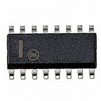
IC MUX/DEMUX 8X1 16SOIC

MC74HC4851ADR2G

Manufacturer Part Number
MC74HC4851ADR2G
Description
IC MUX/DEMUX 8X1 16SOIC
Manufacturer
ON Semiconductor
Series
74HCr
Type
Analog Multiplexerr
Datasheet

Specifications of MC74HC4851ADR2G

Function
Multiplexer/Demultiplexer
Circuit
1 x 8:1
On-state Resistance
600 Ohm
Voltage Supply Source
Single Supply
Voltage - Supply, Single/dual (±)
2 V ~ 6 V
Current - Supply
20µA
Operating Temperature
-55°C ~ 125°C
Mounting Type
Surface Mount
Package / Case
16-SOIC (0.154", 3.90mm Width)
Multiplexer Configuration
Single 8:1
Number Of Inputs
8
Number Of Outputs
1
Number Of Channels
1
Analog Switch On Resistance
1700@2VOhm
Analog Switch Turn On Time
260ns
Analog Switch Turn Off Time
260ns
Package Type
SOIC
Power Supply Requirement
Single
Single Supply Voltage (min)
2V
Single Supply Voltage (typ)
3/5V
Single Supply Voltage (max)
6V
Dual Supply Voltage (min)
Not RequiredV
Dual Supply Voltage (typ)
Not RequiredV
Dual Supply Voltage (max)
Not RequiredV
Power Dissipation
500mW
Mounting
Surface Mount
Pin Count
16
Operating Temp Range
-55C to 125C
Operating Temperature Classification
Military
Lead Free Status / RoHS Status
Lead free / RoHS Compliant
Other names
MC74HC4851ADR2GOS
MC74HC4851ADR2GOS
MC74HC4851ADR2GOSTR

Available stocks

Company
Part Number
Manufacturer
Quantity
Price
Part Number:
MC74HC4851ADR2G
Manufacturer:
ON Semiconductor
Quantity:
8 850
Part Number:
MC74HC4851ADR2G
Manufacturer:
ON/安森美
Quantity:
20 000
MC74HC4851A,
MC74HC4852A
Analog Multiplexers/
Demultiplexers with
Injection Current Effect
Control
Automotive Customized
MC1405xB analog mux/demux devices, but feature injection current
effect control. This makes them especially suited for usage in
automotive applications where voltages in excess of normal logic
voltage are common.
input channels to exceed the supply voltage range without affecting
the signal of the enabled analog channel. This eliminates the need for
external diode/ resistor networks typically used to keep the analog
channel signals within the supply voltage range.
Channel Select and Enable inputs are compatible with standard CMOS
outputs.
Features
*For additional information on our Pb−Free strategy and soldering details, please
© Semiconductor Components Industries, LLC, 2009
October, 2009 − Rev. 8
download the ON Semiconductor Soldering and Mounting Techniques
Reference Manual, SOLDERRM/D.
These devices are pin compatible to standard HC405x and
The injection current effect control allows signals at disabled analog
The devices utilize low power silicon gate CMOS technology. The
Injection Current Cross−Coupling Less than 1mV/mA (See Figure 9)
Pin Compatible to HC405X and MC1405XB Devices
Power Supply Range (V
In Compliance With the Requirements of JEDEC Standard No. 7A
Chip Complexity: 154 FETs or 36 Equivalent Gates
These are Pb−Free Devices*
CC
− GND) = 2.0 to 6.0 V
1
16
16
16
See detailed ordering and shipping information in the package
dimensions section on page 12 of this data sheet.
16
1
1
1
x
A
WL, L
YY, Y
WW, W
G or G
(Note: Microdot may be in either location)
1
ORDERING INFORMATION
http://onsemi.com
SOIC−16 WIDE
CASE 751B
CASE 948F
TSSOP−16
DT SUFFIX
CASE 648
= 1 or 2
= Assembly Location
= Wafer Lot
= Year
= Work Week
= Pb−Free Package
N SUFFIX
D SUFFIX
DW SUFFIX
CASE 751G
SOIC−16
PDIP−16
Publication Order Number:
16
16
1
16
1
1
MC74HC485xAN
MC74HC4851A/D
DIAGRAMS
AWLYYWWG
16
1
MARKING
HC485xAG
AWLYWW
AWLYWWG
HC4851A
ALYWG
HC48
5xA
G

Related parts for MC74HC4851ADR2G

MC74HC4851ADR2G Summary of contents

Page 1

... Chip Complexity: 154 FETs or 36 Equivalent Gates • These are Pb−Free Devices* *For additional information on our Pb−Free strategy and soldering details, please download the ON Semiconductor Soldering and Mounting Techniques Reference Manual, SOLDERRM/D. © Semiconductor Components Industries, LLC, 2009 October, 2009 − Rev. 8 http://onsemi.com PDIP− ...

Page 2

ANALOG 12 MULTIPLEXER/ X3 INPUTS/ 1 DEMULTIPLEXER OUTPUTS CHANNEL 10 B SELECT 9 INPUTS C 6 ENABLE PIN PIN 8 = ...

Page 3

MAXIMUM RATINGS Î Î Î Î Î Î Î Î Î Î Î Î Î Î Î ...

Page 4

DC CHARACTERISTICS — Analog Section Symbol Parameter R Maximum “ON” Resistance on DR Delta “ON” Resistance on I Maximum Off−Channel Leakage Current, off Any One Channel Common Channel I Maximum On−Channel Leakage on Channel−to−Channel AC CHARACTERISTICS ( pF, ...

Page 5

V , INPUT VOLTAGE (VOLTS), REFERENCED TO GND in Figure 5. Typical On Resistance V 660 600 540 480 420 360 300 240 180 ...

Page 6

Vin2 / Iin2 meas. here. Current Source HP4155C Smu #2 RS Vin1 = 4.9 V (Smu3) Iin1 meas. Here Vm1 connected here. GND Figure 9. Injection Current Coupling Specification External DC P. ...

Page 7

V HC4051A Sensor Channel 1 Channel 2 Channel 3 Channel 4 Channel 5 Channel 6 Channel 7 Channel 8 (8x Identical Circuitry) Common Out Figure 10. Actual Technology Requires 32 passive components and one extra 6V regulator to ...

Page 8

PLOTTER PROGRAMMABLE POWER MINI COMPUTER SUPPLY - + DEVICE UNDER TEST ANALOG IN GND Figure 12. On Resistance Test Set− ANALOG I/O OFF V CC OFF Figure 14. Maximum Off Channel ...

Page 9

ANALOG 50 PLH ANALOG 50% OUT Figure 18. Propagation Delays, Analog In to Analog Out ENABLE t t PZL PLZ ANALOG 50% OUT t t PZH PHZ ANALOG 50% OUT Figure 20. Propagation Delays, ...

Page 10

Disabled Analog Mux Input V > Figure 23. Diagram of Bipolar Coupling Mechanism Appears ENABLE Gate = V CC (Disabled ...

Page 11

ENABLE Figure 25. Function Diagram, HC4852A http://onsemi.com 11 INJECTION 13 X0 CURRENT CONTROL INJECTION 14 X1 CURRENT CONTROL INJECTION 15 X2 CURRENT CONTROL INJECTION 12 X3 CURRENT CONTROL INJECTION 13 X CURRENT CONTROL INJECTION 1 ...

Page 12

... ORDERING INFORMATION Device MC74HC4851ANG MC74HC4851ADG MC74HC4851ADR2G MC74HC4851ADTR2G MC74HC4851ADWG MC74HC4851ADWR2G MC74HC4852ANG MC74HC4852ADG MC74HC4852ADR2G MC74HC4852ADTR2G †For information on tape and reel specifications, including part orientation and tape sizes, please refer to our Tape and Reel Packaging Specifications Brochure, BRD8011/D. *This package is inherently Pb−Free. Package PDIP−16 (Pb− ...

Page 13

0.25 (0.010) −A− −T− SEATING PLANE 0.25 (0.010 PACKAGE DIMENSIONS PDIP−16 N SUFFIX CASE 648−08 ...

Page 14

16X 0. 14X K 16X REF 0.10 (0.004) 0.15 (0.006 L PIN 1 IDENT. 1 0.15 (0.006 ...

Page 15

... Opportunity/Affirmative Action Employer. This literature is subject to all applicable copyright laws and is not for resale in any manner. PUBLICATION ORDERING INFORMATION LITERATURE FULFILLMENT: Literature Distribution Center for ON Semiconductor P.O. Box 5163, Denver, Colorado 80217 USA Phone: 303−675−2175 or 800−344−3860 Toll Free USA/Canada Fax: 303− ...

Related keywords