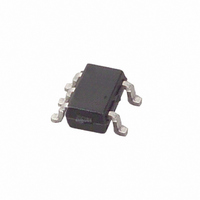
MAX4595EXK+T Maxim Integrated Products, MAX4595EXK+T Datasheet - Page 6

MAX4595EXK+T
Manufacturer Part Number
MAX4595EXK+T
Description
IC SWITCH SPST SC70-5
Manufacturer
Maxim Integrated Products
Datasheet
1.MAX4594EXKT.pdf
(10 pages)
Specifications of MAX4595EXK+T
Function
Switch
Circuit
1 x SPST- NC
On-state Resistance
10 Ohm
Voltage Supply Source
Single Supply
Voltage - Supply, Single/dual (±)
2 V ~ 5.5 V
Current - Supply
1µA
Operating Temperature
-40°C ~ 85°C
Mounting Type
Surface Mount
Package / Case
6-TSSOP (5 lead), SC-88A, SOT-353
Lead Free Status / RoHS Status
Lead free / RoHS Compliant
Low-Voltage, Single-Supply,
10Ω SPST CMOS Analog Switches
Analog signals can range over the supply voltage (V+ to
GND) with on-resistance changing very little over the
entire range (see Typical Operating Characteristics). The
MAX4594–MAX4597 are bidirectional, so the NO, NC,
and COM pins can be used either as inputs or outputs.
Figure 1. Overvoltage Protection Using Two External Blocking
Diodes
6
Figure 2. Charge Injection
_______________________________________________________________________________________
V g
V
IN
Applications Information
50Ω
IN
NO
OR
NC
POSITIVE SUPPLY
MAX4594
MAX4595
MAX4596
MAX4597
GND
V+
GND
V+
V+
Analog Signal Levels
D1
D2
COM
COM
NO
NC
or
V
NO
C
1000pF
L
or V
V
OUT
NC
= 0
Proper power-supply sequencing is recommended for
all CMOS devices. Always apply V+ before applying
analog signals or logic inputs, especially if the analog
or logic signals are not current limited. If this sequenc-
ing is not possible, and if the analog or logic inputs are
not current limited to <20mA, add a small-signal diode
(D1) as shown in Figure 1. If the analog signal can dip
below GND, add D2. Adding protection diodes
reduces the analog signal range to a diode drop (about
0.7V) below V+ for D1 or to a diode drop above ground
for D2. The addition of diodes does not affect leakage.
On-resistance increases by a small amount at low sup-
ply voltages. Maximum supply voltage (V+) must not
exceed 6V.
Protection diodes D1 and D2 also protect against some
overvoltage situations. A fault voltage up to the absolute
maximum rating at an analog signal input does not dam-
age the device, even if the supply voltage is below the
signal voltage.
V
V
OUT
IN
V+
0V
Test Circuits/Timing Diagrams
∆V
ERROR Q WHEN THE CHANNEL TURNS OFF.
Q = ∆V
OUT
IS THE MEASURED VOLTAGE DUE TO CHARGE TRANSFER
OUT
x C
Power-Supply Sequencing and
L
MAX4594/MAX4596
Overvoltage Protection
MAX4595/MAX4597
∆V
OUT


