NLAS9431MTR2G ON Semiconductor, NLAS9431MTR2G Datasheet
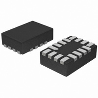
IC SWITCH DUAL DPDT 16WQFN

NLAS9431MTR2G

Manufacturer Part Number
NLAS9431MTR2G
Description
IC SWITCH DUAL DPDT 16WQFN
Manufacturer
ON Semiconductor
Datasheet

Specifications of NLAS9431MTR2G

Function
Switch
Circuit
2 x DPDT
On-state Resistance
30 Ohm
Voltage Supply Source
Single Supply
Voltage - Supply, Single/dual (±)
2 V ~ 5.5 V
Current - Supply
4µA
Operating Temperature
-55°C ~ 125°C
Mounting Type
Surface Mount
Package / Case
16-WFQFN Exposed Pad
Switch Configuration
DPDT
On Resistance (max)
85 Ohm @ 2.5 V
On Time (max)
35 ns @ 2.5 V
Off Time (max)
12 ns @ 2.5 V
Supply Voltage (max)
5.5 V
Supply Voltage (min)
2 V
Maximum Power Dissipation
800 mW
Maximum Operating Temperature
+ 125 C
Mounting Style
SMD/SMT
Minimum Operating Temperature
- 55 C
Lead Free Status / RoHS Status
Lead free / RoHS Compliant
Other names
NLAS9431MTR2G
NLAS9431MTR2GOSTR

Available stocks

Company
Part Number
Manufacturer
Quantity
Price
Part Number:
NLAS9431MTR2G
Manufacturer:
ON Semiconductor
Quantity:
2 200
Part Number:
NLAS9431MTR2G
Manufacturer:
ON/安森美
Quantity:
20 000
NLAS9431
Low Voltage Single Supply
Dual DPDT Analog Switch
pole−double throw (DPDT) analog switch fabricated with silicon
gate CMOS technology. It achieves high speed propagation delays
and low ON resistances while maintaining CMOS low power
dissipation. This DPDT controls analog and digital voltages that may
vary across the full power−supply range (from V
lower and more linear over input voltage than R
analog switches.
voltages between 0 V and 5.5 V are applied, regardless of the supply
voltage. This input structure helps prevent device destruction caused
by supply voltage − input/output voltage mismatch, battery backup,
hot insertion, etc.
demultiplexer analog switch with two Select pins that each controls
two multiplexer−demultiplexers.
© Semiconductor Components Industries, LLC, 2008
July, 2008 − Rev. 1
The NLAS9431 is an advanced dual−independent CMOS double
The device has been designed so the ON resistance (R
The channel select input is compatible with standard CMOS outputs.
The channel select input structure provides protection when
The NLAS9431 can also be used as a quad 2−to−1 multiplexer−
Direct Battery Connection
Channel Select Input Over−Voltage Tolerant to 5.5 V
Fast Switching and Propagation Speeds
Break−Before−Make Circuitry
Low Power Dissipation: I
Diode Protection Provided on Channel Select Input
Improved Linearity and Lower ON Resistance over Input Voltage
Latch−up Performance Exceeds 300 mA
Chip Complexity: 158 FETs
16−Lead WQFN Package, 1.8 mm x 2.6 mm
This is a Pb−Free Device
CC
= 2 mA (Max) at T
ON
CC
A
of typical CMOS
to GND).
= 25°C
ON
) is much
1
See detailed ordering and shipping information in the package
dimensions section on page 10 of this data sheet.
BA
M
G
CASE 488AP
WQFN16
ORDERING INFORMATION
http://onsemi.com
= Specific Device Code
= Date Code & Assembly Location
= Pb−Free Device
Publication Order Number:
1
Î Î
DIAGRAMS
16
MARKING
B A M
G
NLAS9431/D

Related parts for NLAS9431MTR2G

NLAS9431MTR2G Summary of contents

Page 1

NLAS9431 Low Voltage Single Supply Dual DPDT Analog Switch The NLAS9431 is an advanced dual−independent CMOS double pole−double throw (DPDT) analog switch fabricated with silicon gate CMOS technology. It achieves high speed propagation delays and low ON resistances while maintaining ...

Page 2

FUNCTION TABLE Select Channel COM COM Figure 1. Logic Diagram SELECT AB U COM A U COM B SELECT CD U COM C U COM D Figure 2. IEC Logic ...

Page 3

MAXIMUM RATINGS Symbol V Positive DC Supply Voltage CC V Analog Input Voltage ( Digital Select Input Voltage Current, Into or Out of Any Pin IK P Power Dissipation in Still Air ...

Page 4

DC CHARACTERISTICS − Digital Section (Voltages Referenced to GND) Symbol Parameter V Minimum High−Level Input IH Voltage, Select Inputs V Maximum Low−Level Input IL Voltage, Select Inputs I Maximum Input Leakage IN Current I Power Off Leakage Current, OFF Select ...

Page 5

AC ELECTRICAL CHARACTERISTICS Symbol Parameter t Turn−On Time ON (Figures 12 and 13) t Turn−Off Time OFF (Figures 12 and 13) t Minimum Break−Before−Make BBM Time C Maximum Input Capacitance, Select Input Analog I/O (switch off) ...

Page 6

DUT V Output IS 0.1 mF 300 W Switch Select Pin DUT V Output IS 0.1 mF Open Input DUT Output Open Input V IS Input GND V OUT 35 pF Output GND Figure 4. t (Time Break−Before−Make) BBM V ...

Page 7

W Generator Channel switch control/s test socket is normalized. Off isolation is measured across an off channel. On loss is the bandwidth switch. V ISO V = Off Channel Isolation = 20 Log ISO V = ...

Page 8

Off Isolation −60 −80 −100 0.01 0.1 1 FREQUENCY (MHz) Figure 10. Off−Channel Isolation (ns (ns) 5 OFF 0 2.5 3 3.5 V (VOLTS) CC Figure 12. t and ...

Page 9

0.001 0.0001 0.00001 −40 − Temperature (°C) Figure 16. I vs. Temp 100 125°C ...

Page 10

... V (VDC) IS Figure 22. R vs. Temp DEVICE ORDERING INFORMATION Circuit Indicator Technology Device NLAS9431MTR2G NL †For information on tape and reel specifications, including part orientation and tape sizes, please refer to our Tape and Reel Packaging Specifications Brochure, BRD8011/D. *This package is inherently Pb−Free 3.5 4.0 4 ...

Page 11

... C NOTE 3 1.200 0.0472 *For additional information on our Pb−Free strategy and soldering details, please download the ON Semiconductor Soldering and Mounting Techniques Reference Manual, SOLDERRM/D. N. American Technical Support: 800−282−9855 Toll Free USA/Canada Europe, Middle East and Africa Technical Support: Phone: 421 33 790 2910 Japan Customer Focus Center Phone: 81− ...

Related keywords