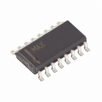
MAX4582CSE Maxim Integrated Products, MAX4582CSE Datasheet - Page 8

MAX4582CSE
Manufacturer Part Number
MAX4582CSE
Description
IC MULTIPLEXER DUAL 4X1 16SOIC
Manufacturer
Maxim Integrated Products
Datasheet
1.MAX4582LEEE.pdf
(18 pages)
Specifications of MAX4582CSE
Function
Multiplexer
Circuit
2 x 4:1
On-state Resistance
80 Ohm
Voltage Supply Source
Single, Dual Supply
Voltage - Supply, Single/dual (±)
2 V ~ 12 V, ±2 V ~ 6 V
Current - Supply
1µA
Operating Temperature
0°C ~ 70°C
Mounting Type
Surface Mount
Package / Case
16-SOIC (0.154", 3.90mm Width)
Lead Free Status / RoHS Status
Contains lead / RoHS non-compliant
Available stocks
Company
Part Number
Manufacturer
Quantity
Price
Company:
Part Number:
MAX4582CSE
Manufacturer:
MAXIM
Quantity:
5
Company:
Part Number:
MAX4582CSE
Manufacturer:
MAXIM
Quantity:
15
Part Number:
MAX4582CSE
Manufacturer:
MAXIM/美信
Quantity:
20 000
Company:
Part Number:
MAX4582CSE+T
Manufacturer:
MAXIM
Quantity:
2
The MAX4581/MAX4582/MAX4583 construction is typi-
cal of most CMOS analog switches. They have three
Low-Voltage, CMOS Analog
Multiplexers/Switches
Note: Input and output pins are identical and interchangeable. Any may be considered an input or output; signals pass equally well
8
__________Applications Information
D IP , S O ,
1, 5, 2, 4
TS S OP
13, 14,
15, 12,
_______________________________________________________________________________________
16
11
10
—
—
—
—
—
—
—
—
—
—
—
3
9
8
7
6
MAX4581
in both directions.
11, 12,
13, 10,
15, 3,
16, 2
QFN
EP
14
—
—
—
—
—
—
—
—
—
—
1
9
8
7
6
5
4
Power-Supply Considerations
D IP , S O ,
TS S OP
12, 14,
1, 5, 2,
15, 11
13
16
10
—
—
—
—
—
—
—
—
—
—
4
3
9
8
7
6
MAX4582
PIN
10, 12,
15, 3,
13, 9
16, 2
QFN
EP
—
11
—
—
—
—
—
—
—
14
—
1
8
7
6
5
4
D IP , S O ,
TS S OP
Overview
14
15
13
12
16
11
10
—
—
—
—
1
2
3
5
4
9
8
7
6
MAX4583
QFN
EP
12
13
11
10
15
16
14
—
—
—
1
3
2
9
8
7
6
5
4
supply pins: V
to drive the internal CMOS switches and set the limits of
the analog voltage on any switch. Reverse ESD-
protection diodes are internally connected between
each analog-signal pin and both V
analog signal exceeds V
ENABLE
X0, X1,
Y0, Y1,
NAME
X0–X7
X2, X3
Y2, Y3
GND
V
V
EP
X1
X0
Y1
Y0
Z1
Z0
C
X
Y
Z
CC
A
B
EE
CC
Analog Switch Inputs 0–7
Analog Switch “X” Output
Analog Switch “X” Inputs 0–3
Analog Switch “Y” Inputs 0–3
Analog Switch “Y” Output
Analog Switch “X” Normally Open Input
Analog Switch “X” Normally Closed Input
Analog Switch “Y” Normally Open Input
Analog Switch “Y” Normally Open Input
Analog Switch “Z” Normally Open Input
Analog Switch “Z” Normally Open Input
Analog Switch “Z” Output
Positive Analog and Digital Supply-Voltage
Input
Digital Address “A” Input
Digital Address “B” Input
Digital Address “C” Input
Ground. Connect to digital ground. (Analog
signals have no ground reference; they are
limited to V
Negative Analog Supply-Voltage Input.
Connect to GND for
single-supply operation.
Digital Enable Input. Normally connected to
GND.
Exposed Pad. Connect EP to V
, V
EE
, and GND. V
CC
CC
and V
or V
FUNCTION
Pin Description
EE
EE
.)
, one of these diodes
CC
CC
and V
and V
CC
.
EE
EE
are used
. If any


