AD8426ACPZ-R7 Analog Devices Inc, AD8426ACPZ-R7 Datasheet - Page 23
AD8426ACPZ-R7
Manufacturer Part Number
AD8426ACPZ-R7
Description
58T4523
Manufacturer
Analog Devices Inc
Specifications of AD8426ACPZ-R7
Rohs Compliant
YES
Lead Free Status / Rohs Status
Compliant


LAYOUT
To ensure optimum performance of the
level, care must be taken in the design of the board layout.
The
this task.
Package Considerations
The
no exposed paddle. The footprint from another 4 mm × 4 mm
LFCSP part should not be copied because it may not have the
correct lead pitch and lead width dimensions. Refer to the
Outline Dimensions section to verify that the corresponding
dimensional symbol has the correct dimensions.
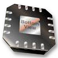
Hidden Paddle Package
The
paddle. Unlike chip scale packages where the pad limits routing
capability, this package allows routes and vias directly beneath
the chip. In this way, the full space savings of the small LFCSP
can be realized. Although the package has no metal in the center
of the part, the manufacturing process leaves a very small section
of exposed metal at each of the package corners, as shown in
Figure 64 and in Figure 73 in the Outline Dimensions section.
This metal is connected to −V
possibility of a short, vias should not be placed beneath these
exposed metal tabs.
AD8426
AD8426
AD8426
Figure 64. Hidden Paddle Package, Bottom View
NOTES
1. EXPOSED METAL TABS AT THE FOUR
is available in a 16-lead, 4 mm × 4 mm LFCSP with
pins are arranged in a logical manner to aid in
is available in an LFCSP package with a hidden
–IN1
+IN1
RG1
RG1
CORNERS OF THE PACKAGE ARE
INTERNALLY CONNECTED TO –V
1
2
3
4
AD8426
BOTTOM VIEW
Figure 63. Pinout Diagram
16
5
15
6
S
14
through the part. Because of the
7
13
8
HIDDEN
PADDLE
EXPOSED METAL
TABS
S
AD8426
.
12
11
10
9
–IN2
RG2
RG2
+IN2
at the PCB
Rev. 0 | Page 23 of 28
Common-Mode Rejection Ratio over Frequency
Poor layout can cause some of the common-mode signals to be
converted to differential signals before reaching the in-amp. Such
conversions occur when one input path has a frequency response
that is different from the other. To keep CMRR over frequency
high, the input source impedance and capacitance of each path
should be closely matched. Additional source resistance in the
input paths (for example, for input protection) should be placed
close to the in-amp inputs to minimize the interaction of the
inputs with parasitic capacitance from the PCB traces.
Parasitic capacitance at the gain setting pins can also affect CMRR
over frequency. If the board design has a component at the gain
setting pins (for example, a switch or jumper), the component
should be chosen so that the parasitic capacitance is as small as
possible.
Power Supplies
A stable dc voltage should be used to power the instrumenta-
tion amplifier. Noise on the supply pins can adversely affect
performance. See the PSRR performance curves in Figure 22
and Figure 25 for more information.
A 0.1 μF capacitor should be placed as close as possible to each
supply pin. As shown in Figure 65, a 10 μF capacitor can be used
farther away from the part. In most cases, it can be shared by
other precision integrated circuits.
References
The output voltage of the
the potential on the reference terminal. Care should be taken to
tie the REFx pins to the appropriate local ground. This should
also help minimize crosstalk between the two channels.
Figure 65. Supply Decoupling, REF, and Output Referred to Local Ground
R
G
+IN
–IN
AD8426
AD8426
+V
–V
S
S
0.1µF
0.1µF
REF
is developed with respect to
10µF
10µF
LOAD
OUT
AD8426
Related parts for AD8426ACPZ-R7
Image
Part Number
Description
Manufacturer
Datasheet
Request
R

Part Number:
Description:
Wideband, High Output Current, Fast Settling Op Amp
Manufacturer:
Analog Devices

Part Number:
Description:
±1.7g Dual-Axis IMEMS Accelerometer Evaluation Board
Manufacturer:
Analog Devices Inc
Datasheet:

Part Number:
Description:
Inertial Sensor Evaluation System
Manufacturer:
Analog Devices Inc
Datasheet:
Part Number:
Description:
Manufacturer:
Analog Devices Inc
Datasheet:
Part Number:
Description:
Manufacturer:
Analog Devices Inc
Datasheet:
Part Number:
Description:
Manufacturer:
Analog Devices Inc
Datasheet:
Part Number:
Description:
Manufacturer:
Analog Devices Inc
Datasheet:
Part Number:
Description:
Manufacturer:
Analog Devices Inc
Datasheet:
Part Number:
Description:
Manufacturer:
Analog Devices Inc
Datasheet:
Part Number:
Description:
Manufacturer:
Analog Devices Inc
Datasheet:
Part Number:
Description:
Manufacturer:
Analog Devices Inc
Datasheet:
Part Number:
Description:
Manufacturer:
Analog Devices Inc
Datasheet:
Part Number:
Description:
Manufacturer:
Analog Devices Inc
Datasheet: