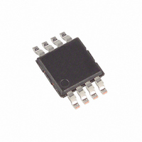
MAX4644EUA Maxim Integrated Products, MAX4644EUA Datasheet - Page 7

MAX4644EUA
Manufacturer Part Number
MAX4644EUA
Description
IC SWITCH SPDT 8UMAX
Manufacturer
Maxim Integrated Products
Datasheet
1.MAX4644EUTT.pdf
(10 pages)
Specifications of MAX4644EUA
Function
Switch
Circuit
1 x SPDT
On-state Resistance
4 Ohm
Voltage Supply Source
Single Supply
Voltage - Supply, Single/dual (±)
1.8 V ~ 5.5 V
Current - Supply
1µA
Operating Temperature
-40°C ~ 85°C
Mounting Type
Surface Mount
Package / Case
8-TSSOP, 8-MSOP (0.118", 3.00mm Width)
Lead Free Status / RoHS Status
Contains lead / RoHS non-compliant
Available stocks
Company
Part Number
Manufacturer
Quantity
Price
Company:
Part Number:
MAX4644EUA
Manufacturer:
MAXIM
Quantity:
26
Part Number:
MAX4644EUA
Manufacturer:
MAXIM/美信
Quantity:
20 000
The MAX4644 operates from a single supply ranging
from +1.8V to +5.5V. The device is guaranteed to be
functional over that supply range, but TTL/CMOS com-
patibility is only valid for operation using a +5V supply.
All voltage levels are referenced to GND. Positive and
negative DC analog inputs or AC signals can be
accommodated by shifting V+ and GND.
ESD-protection diodes are internally connected
between each analog-signal pin and both V+ and GND.
One of these diodes conducts if any analog signal
exceeds V+ or GND (Figure 1). Virtually all of the ana-
log leakage current comes from the ESD diodes to V+
Figure 1. Overvoltage Protection Using External Blocking
Diodes
N0, NC
Applications Information
_______________________________________________________________________________________
GND
V+
COM
High-Speed, Low-Voltage, 4 Ω ,
SPDT CMOS Analog Switch
or GND. Although the ESD diodes on a given signal pin
are identical, and therefore fairly well balanced, they
are reverse biased differently. Each is biased by either
V+ or GND and the analog signal. This means their
leakages will vary as the signal varies. The difference in
the two diode leakages to the V+ and GND pins consti-
tutes the analog-signal-path leakage current. All analog
leakage current flows between each pin and one of the
supply terminals, not to the other switch terminal. This is
why both sides of a given switch can show leakage cur-
rents of the same or opposite polarity.
There is no normal current path between the analog-
signal paths and V+ or GND. V+ and GND also power
the internal logic and logic-level translators. The logic-
level translators convert the logic level into switched V+
and GND signals to drive the analog signal gates.
PROCESS: BiCMOS
For the latest package outline information and land patterns
(footprints), go to www.maxim-ic.com/packages. Note that a
“+”, “#”, or “-” in the package code indicates RoHS status only.
Package drawings may show a different suffix character, but
the drawing pertains to the package regardless of RoHS status.
PACKAGE
6 SOT23
8 μMAX
TYPE
PACKAGE
CODE
U6+4
U8+1
Package Information
Chip Information
OUTLINE
21-0058
21-0036
NO.
PATTERN NO.
90-0175
90-0092
LAND
7


