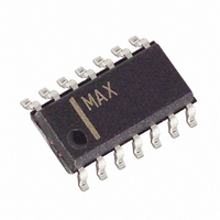
MAX4610CSD+T Maxim Integrated Products, MAX4610CSD+T Datasheet - Page 7

MAX4610CSD+T
Manufacturer Part Number
MAX4610CSD+T
Description
IC SWITCH QUAD SPST 14SOL
Manufacturer
Maxim Integrated Products
Datasheet
1.MAX4612CSD.pdf
(11 pages)
Specifications of MAX4610CSD+T
Function
Switch
Circuit
4 x SPST - NO
On-state Resistance
100 Ohm
Voltage Supply Source
Single Supply
Voltage - Supply, Single/dual (±)
2 V ~ 12 V
Current - Supply
1µA
Operating Temperature
0°C ~ 70°C
Mounting Type
Surface Mount
Package / Case
14-SOIC (0.154", 3.90mm Width)
Lead Free Status / RoHS Status
Lead free / RoHS Compliant
Do not exceed the absolute maximum ratings, because
stresses beyond the listed ratings may cause permanent
damage to the devices.
Proper power-supply sequencing is recommended for all
CMOS devices. Always apply V+ before applying analog
signals or logic inputs, especially if the analog or logic
signals are not current limited. If this sequencing is not
possible, and if the analog or logic inputs are not current
limited to 20mA, add a small-signal diode (D1) as shown
in Figure 1. If the analog signal can dip below GND, add
D2. Adding protection diodes reduces the analog signal
range to a diode drop (about 0.7V) below V+ (for D1),
and to a diode drop above ground (for D2). Leakage is
unaffected by adding the diodes. On-resistance increas-
es by a small amount at low supply voltages. Maximum
supply voltage (V+) must not exceed 13V.
Adding protection diodes causes the logic thresholds to
be shifted relative to the power-supply rails. This can be
TSSOP/SO/ DIP
13, 5, 6, 12
1, 3, 8, 11
2, 4, 9, 10
—
—
—
—
14
—
7
MAX4610
Applications Information
12, 15
14, 5,
8, 11
9, 10
6, 13
QFN
1, 3,
2, 4,
_______________________________________________________________________________________
16
—
—
—
—
7
and Overvoltage Protection
Power-Supply Sequencing
TSSOP/SO/DIP
13, 5, 6, 12
1, 3, 8, 11
2, 4, 9, 10
14
—
—
—
—
—
7
MAX4611
PIN
12, 15
14, 5,
8, 11
9, 10
6, 13
QFN
1, 3,
2, 4,
—
—
16
—
—
7
TSSOP/SO/DIP
13, 5, 6, 12
2, 4, 9, 10
3, 11
1, 8
Low-Voltage, Quad, SPST
—
—
—
14
—
7
MAX4612
CMOS Analog Switches
significant when low supply voltages (+5V or less) are
used. With a +5V supply, TTL compatibility is not guar-
anteed when protection diodes are added. Driving IN1
and IN2 all the way to the supply rails (i.e., to a diode
drop higher than the V+ pin, or to a diode drop lower
than the GND pin) is always acceptable.
Figure 1. Overvoltage Protection Using Two External Blocking
Diodes
12, 15
14, 5,
3, 11
9, 10
6, 13
QFN
2, 4,
1, 8
16
—
—
—
V g
7
COM1–COM4
NO1–NO4
NC1–NC4
NO1, NO3
NC2, NC4
IN1–IN4
NAME
GND
N.C.
V+
EP
NO_
POSITIVE SUPPLY
Analog Switch Normally Open
Terminals
Analog Switch Normally Closed
Terminals
Analog Switch Normally Open
Terminals
Analog Switch Normally Closed
Terminals
Analog Switch Common
Terminals
Logic-Control Digital Input
Ground. Connect to digital
ground.
No Connection. Not internally
connected.
Positive Analog and Digital-
Supply Voltage Input. Internally
connected to substrate.
Exposed Pad (QFN only).
Connect to V+.
V+
Pin Description
COM_
FUNCTION
MAX4610
MAX4611
MAX4612
7


