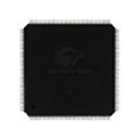
CY7C09569V-83AC Cypress Semiconductor Corp, CY7C09569V-83AC Datasheet - Page 13

CY7C09569V-83AC
Manufacturer Part Number
CY7C09569V-83AC
Description
Manufacturer
Cypress Semiconductor Corp
Datasheet
1.CY7C09569V-83AC.pdf
(32 pages)
Specifications of CY7C09569V-83AC
Density
576Kb
Access Time (max)
18ns
Sync/async
Synchronous
Architecture
SDR
Clock Freq (max)
45MHz
Operating Supply Voltage (typ)
3.3V
Address Bus
14b
Package Type
TQFP
Operating Temp Range
0C to 70C
Number Of Ports
2
Supply Current
360mA
Operating Supply Voltage (min)
3.135V
Operating Supply Voltage (max)
3.465V
Operating Temperature Classification
Commercial
Mounting
Surface Mount
Pin Count
144
Word Size
36b
Number Of Words
16K
Lead Free Status / Rohs Status
Not Compliant
Available stocks
Company
Part Number
Manufacturer
Quantity
Price
Company:
Part Number:
CY7C09569V-83AC
Manufacturer:
CYPRESS
Quantity:
717
Switching Waveforms
Bank Select Pipelined Read
Left Port Write to Flow-Through Right Port Read
Notes
Document Number: 38-06054 Rev. *D
ADDRESS
ADDRESS
21. In this depth expansion example, B1 represents Bank #1 and B2 is Bank #2; Each Bank consists of one Cypress dual-port device from this data sheet.
22. B0 = B1 = B2 = B3 = BM = SIZE = ADS = CNTEN = V
23. The same waveforms apply for a right port write to flow-through left port read.
24. CE = B0 = B1 = B2 = B3 = ADS = CNTEN=V
25. OE = V
26. If t
DATA
DATA
ADDRESS
ADDRESS
DATA
ADDRESS
until t
CCS
DATA
OUT(B2)
OUT(B1)
CE
CE
CCS
CLK
CLK
R/W
CLK
R/W
maximum specified, then data from right port READ is not valid until the maximum specified for t
OUTR
IL
(B1)
(B1)
(B2)
(B2)
for the right port, which is being read from. OE = V
INL
+ t
(B1)
L
R
R
R
L
L
L
CD1
= ADDRESS
(t
t
t
t
t
SC
SC
SA
SA
CWDD
t
t
t
does not apply in this case).
SW
SD
SA
A
A
(B2)
0
0
t
CH2
MATCH
.
VALID
t
t
t
t
SW
SA
t
t
t
t
MATCH
(continued)
CYC2
CCS
HA
HC
HA
HC
[21, 22]
t
DC
t
CL2
t
t
t
HW
HA
t
t
HW
HA
HD
IL
; CNTRST= V
A
A
1
1
t
CWDD
t
IL
CD2
, CNTRST = V
t
CD1
IH
IH
t
.
for the left port, which is being written to.
SC
Q
t
0
SC
[22, 23, 24, 25, 26]
IH
A
.
A
2
2
t
t
DC
HC
t
HC
t
CD2
MATCH
VALID
NO
Q
MATCH
A
A
1
3
t
NO
3
DC
t
t
CKLZ
CKHZ
t
t
CD2
DC
CWDD
. If t
CCS
t
CD1
>maximum specified, then data is not valid
A
Q
A
4
2
4
t
t
t
CKHZ
CD2
CKLZ
Q
CY7C09569V
CY7C09579V
3
A
A
VALID
5
t
5
t
t
CKLZ
CKHZ
CD2
Page 13 of 32
Q
4
[+] Feedback


