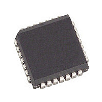
CY7C344-20JC Cypress Semiconductor Corp, CY7C344-20JC Datasheet

CY7C344-20JC
Specifications of CY7C344-20JC
Available stocks
Related parts for CY7C344-20JC
CY7C344-20JC Summary of contents
Page 1
... All inputs, macrocells, and I/O pins are interconnected within the LAB. The speed and density of the CY7C344 makes it a natural for all types of applications. With just this one device, the designer can implement complex state machines, registered logic, and combinatorial “ ...
Page 2
... MHz 2.0V 1.0 MHz OUT [7] R1 464Ω 250Ω (b) 1.75V = 5V. and t , which is used for part ( Test Load and Waveforms. All external timing ER XZ FOR CY7C344 [2] .........................................–3.0V to +7.0V Ambient Temperature ° ° +70 C ° ° – +85 C ° ° – +125 C (Case) Min ...
Page 3
... GND. For the most device when driving subsequent registered logic with a positive hold time and using the same clock as the CY7C344. In general greater than the minimum required input hold time of the subse- quent logic (synchronous or asynchronous), then the devices are ...
Page 4
... Com’l/Ind Mil Com’l/Ind Mil [7] Com’l/Ind Mil [4] Com’l/Ind Mil [4] Com’l/Ind Mil [4] Com’l/Ind Mil [4] Com’l/Ind Mil Com’l/Ind Mil [4] Com’l /Ind Mil [4] Com’l /Ind Mil FOR CY7C344 [7] 7C344-15 7C344-20 7C344-25 Min. Max. Min. Max. Min ...
Page 5
... Com’l /Ind Mil [4] ) Com’l/Ind MAX3 Mil [4, 14 Com’l/Ind CO1 S Mil Com’l/Ind [4, 15] Mil Com’l/Ind [4, 16] ) CO1 Mil Com’l/Ind Mil Com’l/Ind Mil FOR CY7C344 [7] 7C344-15 7C344-20 7C344-25 Min. Max. Min. Max. Min 50.0 41.6 33.3 50 ...
Page 6
... Com’l/Ind Mil Com’l/Ind [4, 25] ) Mil Com’l/Ind Mil should be used for both t AWH + 1 also indicates the maximum frequency at which the device may operate in the asynchronously clocked AS AH ACO1 FOR CY7C344 [7] 7C344-15 7C344-20 7C344-25 Min. Max. Min. Max. Min. Max ...
Page 7
... Mil Com’l/Ind Mil Com’l/Ind Mil Com’l/Ind Mil [28] Com’l/Ind Mil Com’l/Ind Mil Com’l/Ind Mil Com’l/Ind Mil Com’l/Ind Mil Com’l/Ind Mil Com’l/Ind Mil FOR CY7C344 [7] 7C344-15 7C344-20 7C344-25 Min. Max. Min. Max. Min ...
Page 8
... REGISTERED FEEDBACK Document #: 38-03006 Rev. *B USE ULTRA37000 TM ALL NEW DESIGNS Over Operating Range Description Com’l/Ind Mil Com’l/Ind Mil Mil t /t PD1 PD2 CO1 CO2 FOR CY7C344 [7] (continued) 7C344-15 7C344-20 7C344-25 Min. Max. Min. Max. Min HIGH-IMPEDANCE THREE-STATE VALID OUTPUT Max ...
Page 9
... COMBINATORIAL OUTPUT FROM ASYNCH. REGISTERED [19] FEEDBACK Internal Combinatorial INPUT PIN I/O PIN EXPANDER ARRAY DELAY LOGIC ARRAY INPUT LOGIC ARRAY OUTPUT Document #: 38-03006 Rev. *B USE ULTRA37000 FOR TM ALL NEW DESIGNS ACO1 AOH ACO2 PIA EXP CY7C344 t t AWH AWL LAC LAD Page ...
Page 10
... SYSTEM CLOCK AT REGISTER t RSU DATA FROM LOGIC ARRAY Internal Synchronous (Output Path) CLOCK FROM LOGIC ARRAY DATA FROM LOGIC ARRAY OUTPUT PIN Document #: 38-03006 Rev. *B USE ULTRA37000 TM ALL NEW DESIGNS t AWL RSU LATCH FD t PIA ICS FOR CY7C344 CLR PRE HIGH Z Page ...
Page 11
... Ordering Information Speed (ns) Ordering Code 15 CY7C344-15HC/HI CY7C344-15JC/JI CY7C344-15PC/PI CY7C344-15WC/WI 20 CY7C344-20HC/HI CY7C344-20JC/JI CY7C344-20PC/PI CY7C344-20WC/WI CY7C344-20HMB CY7C344-20WMB 25 CY7C344-25HC/HI CY7C344-25JC/JI CY7C344-25PC/PI CY7C344-25WC/WI CY7C344-25HMB CY7C344-25WMB MILITARY SPECIFICATIONS Group A Subgroup Testing DC Characteristics Parameter CC1 Document #: 38-03006 Rev. *B USE ULTRA37000 FOR TM ALL NEW DESIGNS Package Name Package Type ...
Page 12
... Package Diagrams Document #: 38-03006 Rev. *B USE ULTRA37000 FOR TM ALL NEW DESIGNS 28-Pin Windowed Leaded Chip Carrier H64 CY7C344 51-80077-** Page ...
Page 13
... SEE LEAD END OPTION LEAD END OPTION (LEAD #1, 14, 15 & 28) FOR 51-85001-*A DIMENSIONS IN INCHES [MM] MIN. MAX. REFERENCE JEDEC MO-095 PACKAGE WEIGHT: 2.15 gms SEATING PLANE 0.290[7.36] 0.325[8.25] 0.009[0.23] 3° MIN. 0.012[0.30] 0.310[7.87] 0.385[9.78] CY7C344 51-85014-*D Page ...
Page 14
... The inclusion of Cypress products in life-support systems application implies that the manufacturer assumes all risk of such use and in doing so indemnifies Cypress against all charges. USE ULTRA37000 FOR TM ALL NEW DESIGNS 28-Lead (300-Mil) Windowed CerDIP W22 MIL-STD-1835 D-15 Config. A CY7C344 51-80087-** Page ...
Page 15
... Document History Page Document Title: CY7C344 32-Macrocell MAX® EPLD Document Number: 38-03006 REV. ECN NO. Issue Date ** 106271 04/19/01 *A 213375 See ECN *B 373715 See ECN Document #: 38-03006 Rev. *B USE ULTRA37000 FOR TM ALL NEW DESIGNS Orig. of Change Description of Change SZV Change from Spec number: 38-00127 to 38-03006 FSG Added note to title page: “ ...


