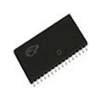
CY62148DV30LL-70ZSXI Cypress Semiconductor Corp, CY62148DV30LL-70ZSXI Datasheet

CY62148DV30LL-70ZSXI
Specifications of CY62148DV30LL-70ZSXI
Available stocks
Related parts for CY62148DV30LL-70ZSXI
CY62148DV30LL-70ZSXI Summary of contents
Page 1
... Note: 1. For best practice recommendations, refer to the Cypress application note “System Design Guidelines” on Cypress Semiconductor Corporation Document #: 38-05341 Rev. *D 4-Mbit (512K x 8) MoBL Functional Description The CY62148DV30 is a high-performance CMOS static RAM organized as 512K words by 8 bits. This device features advanced circuit design to provide ultra-low active current. This is ideal for providing More Battery Life™ ...
Page 2
... CY62148DV30L Industrial 2.2 CY62148DV30LL Industrial CY62148DV30LL Industrial CY62148DV30LL Automotive-A Notes pins are not connected on the die. 3. DNU pins have to be left floating or tied to Vss to ensure proper application. 4. Typical values are included for reference only and are not guaranteed or tested. Typical values are measured at V Document #: 38-05341 Rev ...
Page 3
... Output Current into Outputs (LOW)............................. 20 mA Static Discharge Voltage.......................................... > 2001V (per MIL-STD-883, Method 3015) Latch-up Current..................................................... > 200 mA Operating Range Product + 0.3V CC(max) CY62148DV30L CY62148DV30LL + 0.3V CC(max) CY62148DV30LL Automotive-A –40°C to +85°C + 0.3V CC(max) Test Conditions Min Typ = 2.20V 2 2.70V 2 2.20V ...
Page 4
Capacitance [8] (for all packages) Parameter Description C Input Capacitance IN C Output Capacitance OUT Thermal Resistance Parameter Description Θ Thermal Resistance JA (Junction to Ambient) Θ Thermal Resistance JC (Junction to Case) AC Test Loads and Waveforms R1 V ...
Page 5
Switching Characteristics (Over the Operating Range) Parameter Description Read Cycle t Read Cycle Time RC t Address to Data Valid AA t Data Hold from Address Change OHA t CE LOW to Data Valid ACE t OE LOW to Data ...
Page 6
Switching Waveforms (continued) [15, 16] Read Cycle No. 2 (OE Controlled) ADDRESS CE t ACE OE t LZOE HIGH IMPEDANCE DATA OUT t LZCE SUPPLY CURRENT [17, 18] Write Cycle No. 1 (WE Controlled) ADDRESS CE ...
Page 7
Switching Waveforms (continued) [17, 18] Write Cycle No. 2 (CE Controlled) ADDRESS DATA IO Write Cycle No. 3 (WE Controlled, OE LOW) ADDRESS NOTE 19 DATA IO t HZWE Truth Table CE WE ...
Page 8
... Ordering Information Speed (ns) Ordering Code 55 CY62148DV30LL-55BVI CY62148DV30LL-55BVXI CY62148DV30L-55ZSXI CY62148DV30LL-55ZSXI CY62148DV30LL-55SXI 70 CY62148DV30LL-70ZSXI CY62148DV30LL-70ZSXA 51-85095 32-pin TSOP II (Pb-free) Contact your local Cypress sales representative for availability of these parts Package Diagrams Figure 1. 36-ball VFBGA ( mm), 51-85149 TOP VIEW A1 CORNER 6.00±0.10 SEATING PLANE C Document #: 38-05341 Rev. *D ...
Page 9
... Document #: 38-05341 Rev. *D © Cypress Semiconductor Corporation, 2006-2007. The information contained herein is subject to change without notice. Cypress Semiconductor Corporation assumes no responsibility for the use of any circuitry other than circuitry embodied in a Cypress product. Nor does it convey or imply any license under patent or other rights. Cypress products are not warranted nor intended to be used for medical, life support, life saving, critical control or safety applications, unless pursuant to an express written agreement with Cypress ...
Page 10
Document History Page Document Title:CY62148DV30, 4-Mbit (512K x 8) MoBL Document Number: 38-05341 Issue Orig. of REV. ECN NO. Date Change ** 127480 06/17/03 *A 131041 01/23/04 *B 222180 See ECN *C 498575 See ECN *D 729917 See ECN Document ...


