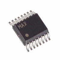
MAX4521EEE Maxim Integrated Products, MAX4521EEE Datasheet

MAX4521EEE
Specifications of MAX4521EEE
Available stocks
Related parts for MAX4521EEE
MAX4521EEE Summary of contents
Page 1
... ON 1 OFF N.C. = NOT CONNECTED Pin Configurations continued at end of data sheet. ________________________________________________________________ Maxim Integrated Products For pricing, delivery, and ordering information, please contact Maxim Direct at 1-888-629-4642, or visit Maxim’s website at www.maxim-ic.com. ♦ +2V to +12V Single Supply ±2V to ±6V Dual Supplies ♦ 100Ω Signal Paths with ±5V Supplies ♦ ...
Page 2
Quad, Low-Voltage, SPST Analog Switches ABSOLUTE MAXIMUM RATINGS Voltages Referenced to GND V+.....................................................................-0.3V to +13.0V V- .....................................................................-13.0V to +0. ............................................................-0.3V to +13.0V All Other Pins (Note 1) ..........................(V- - 0.3V) to (V+ + 0.3V) Continuous Current into ...
Page 3
Quad, Low-Voltage, SPST Analog Switches ELECTRICAL CHARACTERISTICS—Dual Supplies (continued) (V+ = +4.5V to +5.5V -4.5V to -5.5V, T PARAMETER LOGIC INPUT IN_ Input Logic Threshold High IN_ Input Logic Threshold Low IN_ Input Current Logic High I or ...
Page 4
Quad, Low-Voltage, SPST Analog Switches ELECTRICAL CHARACTERISTICS—Single +5V Supply (V+ = +4.5V to +5.5V 0V MIN PARAMETER SYMBOL ANALOG SWITCH V COM_ Analog Signal Range COM_ to NO_, COM_ to NC_ On-Resistance COM_ to ...
Page 5
Quad, Low-Voltage, SPST Analog Switches ELECTRICAL CHARACTERISTICS—Single +3V Supply (V+ = +2.7V to +3.6V 0V MIN PARAMETER ANALOG SWITCH V COM_ Analog Signal Range COM_ to NO_, COM_ to NC_ On-Resistance LOGIC INPUT IN_ ...
Page 6
Quad, Low-Voltage, SPST Analog Switches (V+ = +5V -5V, GND = +25°C, unless otherwise noted.) A ON-RESISTANCE vs. V COM (DUAL SUPPLIES) 180 V 2.0V 160 140 V 3.0V 120 100 ...
Page 7
Quad, Low-Voltage, SPST Analog Switches (V+ = +5V -5V, GND = +25°C, unless otherwise noted.) A TOTAL HARMONIC DISTORTION vs. FREQUENCY 100 -5V 10 600Ω IN AND OUT 1 0.1 ...
Page 8
Quad, Low-Voltage, SPST Analog Switches Applications Information Power-Supply Considerations The MAX4521/MAX4522/MAX4523 construction is typi- cal of most CMOS analog switches. They have three supply pins: V+, V-, and GND. V+ and V- are used to drive the internal CMOS switches, ...
Page 9
Quad, Low-Voltage, SPST Analog Switches MAX4521 V+ MAX4522 MAX4523 V+ COM SWITCH V COM or NC INPUT IN, EN GND V- LOGIC INPUT INCLUDES FIXTURE AND STRAY CAPACITANCE OUT ...
Page 10
Quad, Low-Voltage, SPST Analog Switches V+ 10nF SIGNAL V+ GENERATOR 0dBm COM NC ANALYZER or NO GND R L Figure 4. Off-Isolation V+ 10nF SIGNAL V+ GENERATOR 0dBm COM1 IN1 0 or 2.4V N02 ANALYZER GND Figure ...
Page 11
... Quad, Low-Voltage, SPST Analog Switches Ordering Information (continued) PIN- PART TEMP RANGE PACKAGE MAX4521EPE -40°C to +85°C 16 Plastic DIP MAX4521ESE -40°C to +85°C 16 Narrow SO MAX4521EEE -40°C to +85°C 16 QSOP MAX4521EUE -40°C to +85°C 16 TSSOP MAX4521EGE -40°C to +85°C 16 QFN-EP** MAX4521MJE -55°C to +125°C 16 CERDIP*** MAX4522CPE 0° ...
Page 12
Quad, Low-Voltage, SPST Analog Switches TOP VIEW COM1 IN1 IN2 COM2 NC1 MAX4521 GND 3 10 *EP NC4 COM4 IN4 IN3 COM3 QFN *EP = ...
Page 13
Quad, Low-Voltage, SPST Analog Switches (The package drawing(s) in this data sheet may not reflect the most current specifications. For the latest package outline information www.maxim-ic.com/packages TOP VIEW D e FRONT VIEW ______________________________________________________________________________________ ...
Page 14
Quad, Low-Voltage, SPST Analog Switches (The package drawing(s) in this data sheet may not reflect the most current specifications. For the latest package outline information www.maxim-ic.com/packages.) 14 ______________________________________________________________________________________ Package Information (continued) PACKAGE OUTLINE 12,16,20,24L QFN, 4x4x0. ...
Page 15
... Maxim cannot assume responsibility for use of any circuitry other than circuitry entirely embodied in a Maxim product. No circuit patent licenses are implied. Maxim reserves the right to change the circuitry and specifications without notice at any time. 15 __________________Maxim Integrated Products, 120 San Gabriel Drive, Sunnyvale, CA 94086 (408) 737-7600 © 2007 Maxim Integrated Products Package Information (continued) PACKAGE OUTLINE, TSSOP 4 ...


