MTB33N10E ON Semiconductor, MTB33N10E Datasheet
MTB33N10E
Specifications of MTB33N10E
Available stocks


Related parts for MTB33N10E

MTB33N10E Summary of contents
Page 1
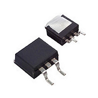
... DS(on) N−Channel PAK CASE 418B 2 1 STYLE 2 3 MARKING DIAGRAM & PIN ASSIGNMENT 4 Drain T33N10E YWW Gate Drain Source T33N10E = Device Code Y = Year WW = Work Week ORDERING INFORMATION Package Shipping 2 D PAK 50 Units/Rail 2 D PAK 800/Tape & Reel Publication Order Number: MTB33N10E/D ...
Page 2
ELECTRICAL CHARACTERISTICS Characteristic OFF CHARACTERISTICS Drain−Source Breakdown Voltage ( Vdc 250 μAdc Temperature Coefficient (Positive) Zero Gate Voltage Drain Current (V = 100 Vdc Vdc 100 Vdc, ...
Page 3
TYPICAL ELECTRICAL CHARACTERISTICS 25° DRAIN−TO−SOURCE VOLTAGE (VOLTS) DS Figure 1. On−Region Characteristics 0.09 ...
Page 4
Switching behavior is most easily modeled and predicted by recognizing that the power MOSFET is charge controlled. The lengths of various switching intervals (Δt) are determined by how fast the FET input capacitance can be charged by current from the ...
Page 5
TOTAL GATE CHARGE (nC) G Figure 8. Gate−To−Source and Drain−To−Source Voltage versus Total Charge DRAIN−TO−SOURCE DIODE CHARACTERISTICS ...
Page 6
SINGLE PULSE T = 25°C 100 C 10 100 μ 1.0 R LIMIT DS(on) 0.1 THERMAL LIMIT PACKAGE LIMIT 0.01 0.1 1 DRAIN−TO−SOURCE VOLTAGE (VOLTS) DS Figure 11. Maximum Rated ...
Page 7
INFORMATION FOR USING THE D RECOMMENDED FOOTPRINT FOR SURFACE MOUNTED APPLICATIONS Surface mount board layout is a critical portion of the total design. The footprint for the semiconductor packages must be the correct size to ensure proper solder connection 0.42 ...
Page 8
Another alternative would be to use a ceramic substrate or an aluminum core board such as Thermal Cladt. Using a board material such as Thermal Clad, an aluminum core Prior to placing surface mount components onto a printed circuit board, ...
Page 9
For any given circuit board, there will be a group of control settings that will give the desired heat pattern. The operator must set temperatures for several heating zones, and a figure for belt speed. Taken together, these control settings ...
Page 10
... J 0.018 0.025 0.46 0.64 K 0.090 0.110 2.29 2.79 S 0.575 0.625 14.60 15.88 V 0.045 0.055 1.14 1.40 STYLE 2: PIN 1. GATE 2. DRAIN 3. SOURCE 4. DRAIN ON Semiconductor Website: www.onsemi.com Order Literature: http://www.onsemi.com/orderlit For additional information, please contact your local Sales Representative MTB33N10E/D ...