VN2406D Vishay, VN2406D Datasheet
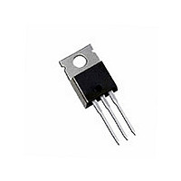
VN2406D

Manufacturer Part Number
VN2406D
Description
Manufacturer
Vishay
Type
Power MOSFETr
Datasheet

Specifications of VN2406D

Number Of Elements
1
Polarity
N
Channel Mode
Enhancement
Drain-source On-res
6Ohm
Drain-source On-volt
240V
Gate-source Voltage (max)
±20V
Continuous Drain Current
1.12A
Power Dissipation
20W
Operating Temp Range
-55C to 150C
Operating Temperature Classification
Military
Mounting
Through Hole
Pin Count
3 +Tab
Package Type
TO-220AB
Lead Free Status / Rohs Status
Not Compliant

Available stocks

Company
Part Number
Manufacturer
Quantity
Price
Part Number:
VN2406D
Manufacturer:
ST
Quantity:
30 000
Notes
a.
b.
c.
Document Number: 70204
S-04279—Rev. F, 16-Jul-01
G
D
S
D Low On-Resistance: 3.5 W
D Secondary Breakdown Free: 260 V
D Low Power/Voltage Driven
D Low Input and Output Leakage
D Excellent Thermal Stability
Drain-Source Voltage
Gate-Source Voltage
Continuous Drain Current
(T
Pulsed Drain Current
Power Dissipation
Thermal Resistance, Junction-to-Ambient
Operating Junction and
Storage Temperature Range
Part Number
J
Pulse width limited by maximum junction temperature.
Reference case for all temperature testing.
Maximum junction-to-case
TO-226AA
= 150_C)
VN2406L
VN2410L
TN2410L
VN2410LS
Top View
VN2406D
TN2410L
VN2406L
VN2410L
(TO-92)
1
2
3
Parameter
a
“S” = Siliconix Logo
xxyy = Date Code
V
’Device Marking
(BR)DSS
TN2410L
VN2406L
VN2410L
Front View
“S” TN
“S” VN
“S” VN
2410L
2406L
2410L
xxyy
xxyy
xxyy
T
T
T
T
240
A
A
A
A
= 25_C
= 100_C
= 25_C
= 100_C
Min (V)
N-Channel 240-V (D-S) MOSFETs
Symbol
T
r
R
D Low Offset Voltage
D Full-Voltage Operation
D Easily Driven Without Buffer
D Low Error Voltage
D No High-Temperature “Run-Away”
J
V
V
DS(on)
10 @ V
10 @ V
10 @ V
I
P
, T
6
DM
thJA
6 @ V
G
I
D
S
DS
GS
D
D
@ V
stg
GS
GS
GS
GS
GS
TO-220AB
1
2
3
Max (W)
(Tab Drain)
Top View
= 10 V
= 10 V
VN2406D
= 4.5 V
= 10 V
= 10 V
TN2410L
_
"20
0.18
0.32
0.11
240
156
0.8
1
TN2410L, VN2406D/L, VN2410L/LS
V
GS(th)
0.5 to 1.8
VN2406D
“S” = Siliconix Logo
xxyy = Date Code
0.8 to 2
0.8 to 2
0.8 to 2
0.8 to 2
’Device Marking
VN2406D
6.25
Front View
"20
1.12
VN2406D
240
0.7
“S” xxyy
20
3
8
(V)
c
b
VN2406L
–55 to 150
"20
0.18
0.11
0.32
240
156
D High-Voltage Drivers: Relays, Solenoids, Lamps,
D Telephone Mute Switches, Ringer Circuits
D Power Supply, Converters
D Motor Control
1.7
0.8
I
D
0.18
1.12
0.18
0.18
0.19
Hammers, Displays, Transistors, etc.
(A)
G
S
D
(Copper Lead Frame)
VN2410LS
VN2410L
Top View
TO-92S
1
2
3
"20
0.18
0.32
0.11
240
156
1.7
0.8
Vishay Siliconix
VN2410LS
"20
0.19
0.12
240
139
0.9
0.4
“S” = Siliconix Logo
xxyy = Date Code
2
’Device Marking
VN2410LS
Front View
www.vishay.com
2410LS
“S” VN
xxyy
Unit
_C/W
_C
W
V
A
11-1

Related parts for VN2406D

VN2406D Summary of contents

Page 1

... A Thermal Resistance, Junction-to-Ambient Operating Junction and Storage Temperature Range Notes a. Pulse width limited by maximum junction temperature. b. Reference case for all temperature testing. c. Maximum junction-to-case Document Number: 70204 S-04279—Rev. F, 16-Jul-01 TN2410L, VN2406D/L, VN2410L/LS r Max (W) V (V) DS(on) GS(th 4.5 V 0 ...

Page 2

... TN2410L, VN2406D/L, VN2410L/LS Vishay Siliconix _ Parameter Symbol Static Drain-Source Breakdown Voltage V (BR)DSS Gate-Threshold Voltage V GS(th) Gate-Body Leakage I GSS Zero Gate Voltage Drain Current I DSS b On-State Drain Current I D(on) b Drain-Source On-Resistance r DS(on) b Forward Transconductance g fs Input Capacitance C iss Output Capacitance C oss Reverse Transfer Capacitance ...

Page 3

... Gate-Source Voltage (V) GS On-Resistance vs. Drain Current 0.1 0.2 0.3 I – Drain Current (A) D Document Number: 70204 S-04279—Rev. F, 16-Jul-01 TN2410L, VN2406D/L, VN2410L/ 4.0 V 3.5 V 3.0 V 2 125_C 25_C 4 5 0.4 0.5 0.6 Vishay Siliconix Output Characteristics for Low Gate Drive 200 ...

Page 4

... TN2410L, VN2406D/L, VN2410L/LS Vishay Siliconix Threshold Region 150_C J 1 25_C 0.1 0.01 0.3 0.7 1.1 V – Gate-to-Source Voltage (V) GS Gate Charge 15 0 12.5 10 120 V DS 7.5 192 V 5.0 2 400 800 1200 Q – Total Gate Charge (pC) g Drive Resistance Effects on Switching 100 ...

Page 5

... Normalized Effective Transient Thermal Impedance, Junction-to-Ambient (TO-226AA) 1 Duty Cycle = 0.5 0.2 0.1 0.05 0.1 0.02 0.01 Single Pulse 0.01 0.1 1 Document Number: 70204 S-04279—Rev. F, 16-Jul-01 TN2410L, VN2406D/L, VN2410L/ 100 t – Square Wave Pulse Duration (sec) 1 Vishay Siliconix Notes Duty Cycle ...

Page 6

... Vishay disclaims any and all liability arising out of the use or application of any product described herein or of any information provided herein to the maximum extent permitted by law. The product specifications do not expand or otherwise modify Vishay’ ...

Related keywords