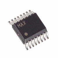
MAX4536EEE Maxim Integrated Products, MAX4536EEE Datasheet - Page 8

MAX4536EEE
Manufacturer Part Number
MAX4536EEE
Description
IC SWITCH QUAD SPST 16QSOP
Manufacturer
Maxim Integrated Products
Datasheet
1.MAX4537ESE.pdf
(12 pages)
Specifications of MAX4536EEE
Function
Switch
Circuit
4 x SPST - NO
On-state Resistance
100 Ohm
Voltage Supply Source
Single, Dual Supply
Voltage - Supply, Single/dual (±)
2 V ~ 12 V, ±2 V ~ 6 V
Current - Supply
1µA
Operating Temperature
-40°C ~ 85°C
Mounting Type
Surface Mount
Package / Case
16-SSOP (0.150", 3.90mm Width)
Lead Free Status / RoHS Status
Contains lead / RoHS non-compliant
Available stocks
Company
Part Number
Manufacturer
Quantity
Price
Company:
Part Number:
MAX4536EEE+
Manufacturer:
Maxim
Quantity:
201
The MAX4536/MAX4537/MAX4538 construction is typi-
cal of most CMOS analog switches. These devices have
three supply pins: V+, V-, and GND. V+ and V- drive the
internal CMOS switches and set the limits of the analog
voltage on any switch. Reverse ESD-protection diodes
are internally connected between each analog-signal
pin, and both V+ and V-. One of these diodes conducts
if any analog signal exceeds V+ or V-. These reverse-
biased ESD diodes leak during normal operation, form-
ing the only current drawn from V+ or V-.
Virtually all the analog leakage current is through the
ESD diodes. Although the ESD diodes on a given sig-
nal pin are identical and therefore fairly well balanced,
they are reverse biased differently. Each is biased by
either V+ or V- and the analog signal. This means their
leakages vary as the signal varies. The difference in the
two diode leakages from the signal path to the V+ and
V- pins constitutes the analog-signal path leakage cur-
rent. All analog leakage current flows to the supply ter-
minals, not to the other switch terminal. This explains
how both sides of a given switch can show leakage
currents of either the same or opposite polarity.
There is no connection between the analog-signal
paths and GND. The analog-signal paths consist of an
N-channel and P-channel MOSFET with their sources
and drains paralleled and their gates driven out of
phase to V+ and V- by the logic-level translators.
V+ and GND power the internal logic and logic-level
translators and set the input logic thresholds. The
logic-level translators convert the logic levels to
switched V+ and V- signals to drive the analog switch-
es’ gates. This drive signal is the only connection
between the logic supplies and the analog supplies.
V+, and V- have ESD-protection diodes to GND. The
logic-level inputs have ESD protection to V+ and to V-.
Increasing V- has no effect on the logic-level thresh-
olds, but it does increase the drive to the P-channel
switches, reducing their on-resistance. V- also sets the
negative limit of the analog-signal voltage.
Quad, Low-Voltage,
SPST Analog Switches with Enable
8
__________Applications Information
_______________________________________________________________________________________
Power-Supply Considerations
Overview
The logic-level thresholds are CMOS/TTL-compatible
when V+ is +5V. The threshold increases slightly as V+
is raised. When V+ reaches +12V, the level threshold is
about 3.1V, above the TTL output high-level minimum
of 2.8V, but still compatible with CMOS outputs.
The MAX4536/MAX4537/MAX4538 operate with bipolar
supplies between ±2.0V and ±6V. The V+ and V- sup-
plies need not be symmetrical, but their sum cannot
exceed the absolute maximum rating of 13.0V. Do not
connect the MAX4536/MAX4537/MAX4538’s V+ to
+3V and then connect the logic-level input pins to
TTL logic-level signals. TTL logic-level outputs in
excess of the absolute maximum ratings can dam-
age the part and/or external circuits.
The MAX4536/MAX4537/MAX4538 operate from single
supplies between +2.0V and +12V when V- is connect-
ed to GND. All of the bipolar precautions must be
observed.
In 50Ω systems, signal response is reasonably flat up
to 50MHz (see Typical Operating Characteristics ).
Above 20MHz, the on-response has several minor
peaks that are highly layout dependent. The problem
with high-frequency operation is not in turning the
switch on, but in turning it off. The off-state switch acts
like a capacitor and passes higher frequencies with
less attenuation. At 10MHz, off-isolation is about -44dB
in 50Ω systems, becoming worse (approximately 20dB
per decade) as frequency increases. Higher circuit
impedances also make off-isolation worse. Adjacent
channel attenuation is about 3dB above that of a bare
IC socket, and is due entirely to capacitive coupling.
CAUTION: The absolute maximum V+ to V- differen-
tial voltage is 13.0V. Typical ±6V or +12V supplies
with ±10% tolerances can be as high as 13.2V. This
voltage can damage the MAX4536/MAX4537/MAX4538.
Even ±5% tolerance supplies may have overshoot or
noise spikes that exceed 13.0V.
High-Frequency Performance
Bipolar Supplies
Single Supplies


