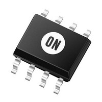
MC33178D ON Semiconductor, MC33178D Datasheet - Page 11

MC33178D
Manufacturer Part Number
MC33178D
Description
Op Amps 2-18V Dual Low Power
Manufacturer
ON Semiconductor
Datasheet
1.MC33178PG.pdf
(19 pages)
Specifications of MC33178D
Number Of Channels
2
Voltage Gain Db
106.02 dB
Common Mode Rejection Ratio (min)
80 dB
Input Voltage Range (max)
Positive Rail - 2 V
Input Voltage Range (min)
Negative Rail + 2 V
Input Offset Voltage
3 mV
Operating Supply Voltage
36 V
Supply Current
0.9 mA
Maximum Operating Temperature
+ 85 C
Mounting Style
SMD/SMT
Package / Case
SOIC-8
Maximum Dual Supply Voltage
+/- 18 V
Minimum Operating Temperature
- 40 C
Lead Free Status / Rohs Status
No
Available stocks
Company
Part Number
Manufacturer
Quantity
Price
Part Number:
MC33178D
Manufacturer:
ON/安森美
Quantity:
20 000
Company:
Part Number:
MC33178DG
Manufacturer:
ON
Quantity:
11 200
Company:
Part Number:
MC33178DG
Manufacturer:
ON
Quantity:
1 479
Part Number:
MC33178DG
Manufacturer:
ON/安森美
Quantity:
20 000
Company:
Part Number:
MC33178DMR2G
Manufacturer:
ON Semiconductor
Quantity:
5
Part Number:
MC33178DMR2G
Manufacturer:
ON/安森美
Quantity:
20 000
Company:
Part Number:
MC33178DR
Manufacturer:
ON
Quantity:
4 722
Company:
Part Number:
MC33178DR2G
Manufacturer:
MOT
Quantity:
10 000
Part Number:
MC33178DR2G
Manufacturer:
ON
Quantity:
20 000
a high output current with a drain current lower than similar
bipolar input op amps. Its 60° phase margin and 15 dB gain
margin ensure stability with up to 1000 pF of load
capacitance (see Figure 24). The ability to drive a minimum
600 W load makes it particularly suitable for telecom
applications. Note that in the sample circuit in Figure 34
both A2 and A3 are driving equivalent loads of
approximately 600 W .
rate and gain bandwidth product make it attractive for a
variety of other applications. For example, although it is not
single supply (the common mode input range does not
include ground), it is specified at +5.0 V with a typical
common mode rejection of 110 dB. This makes it an
excellent choice for use with digital circuits. The high
common mode rejection, which is stable over temperature,
coupled with a low noise figure and low distortion, is an
ideal op amp for audio circuits.
therefore has a certain amount of protection in the event of
a short circuit. However, because of its high current output,
it is especially important not to allow the device to exceed
the maximum junction temperature, particularly with the
This unique device uses a boosted output stage to combine
The low input offset voltage and moderately high slew
The output stage of the op amp is current limited and
Microphone
From
Receiver
To
2.0 k
V
R
120 k
−
+
A2
Figure 34. Telephone Line Interface Circuit
A1
10 k
−
+
APPLICATION INFORMATION
http://onsemi.com
200 k
10 k
11
MC33179 (quad op amp). Shorting more than one amplifier
could easily exceed the junction temperature to the extent of
causing permanent damage.
Stability
dress, component placement, and PC board layout should be
exercised for optimum frequency performance. For
example, long unshielded input or output leads may result in
unwanted input/output coupling. In order to preserve the
relatively low input capacitance associated with these
amplifiers, resistors connected to the inputs should be
immediately adjacent to the input pin to minimize additional
stray input capacitance. This not only minimizes the input
pole frequency for optimum frequency response, but also
minimizes extraneous “pick up” at this node. Supplying
decoupling with adequate capacitance immediately adjacent
to the supply pin is also important, particularly over
temperature, since many types of decoupling capacitors
exhibit great impedance changes over temperature.
capacitances and/or a high source resistance. Simple
compensation schemes can be used to alleviate these
effects.
300
V
R
As usual with most high frequency amplifiers, proper lead
Additional stability problems can be caused by high load
820
−
+
10 k
10 k
1.0 mF
A3
0.05 mF
10 k
1N4678
Tip
Ring
Phone Line


