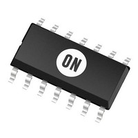
MC74AC74D ON Semiconductor, MC74AC74D Datasheet - Page 2

MC74AC74D
Manufacturer Part Number
MC74AC74D
Description
Flip Flops 2-6V CMOS Dual
Manufacturer
ON Semiconductor
Datasheet
1.MC74AC74DR2G.pdf
(12 pages)
Specifications of MC74AC74D
Number Of Circuits
2
Logic Family
74AC
Logic Type
D-Type Edge Triggered Flip-Flop
Polarity
Inverting/Non-Inverting
Input Type
Single-Ended
Propagation Delay Time
14 ns
High Level Output Current
- 24 mA
Supply Voltage (max)
6 V
Maximum Operating Temperature
+ 85 C
Mounting Style
SMD/SMT
Package / Case
SOIC-14
Minimum Operating Temperature
- 40 C
Supply Voltage (min)
2 V
Dc
08+
Lead Free Status / Rohs Status
No RoHS Version Available
Available stocks
Company
Part Number
Manufacturer
Quantity
Price
Part Number:
MC74AC74DG
Manufacturer:
ON/安森美
Quantity:
20 000
Company:
Part Number:
MC74AC74DR2
Manufacturer:
MOTOROLA
Quantity:
4 453
Part Number:
MC74AC74DR2
Manufacturer:
ON/安森美
Quantity:
20 000
Company:
Part Number:
MC74AC74DTR2
Manufacturer:
ON Semiconductor
Quantity:
1 600
Company:
Part Number:
MC74AC74DTR2G
Manufacturer:
TI
Quantity:
4 600
NOTE:
Stresses exceeding Maximum Ratings may damage the device. Maximum Ratings are stress ratings only. Functional operation above the
Recommended Operating Conditions is not implied. Extended exposure to stresses above the Recommended Operating Conditions may affect
device reliability.
TRUTH TABLE (Each Half)
MAXIMUM RATINGS
V
V
V
I
I
I
T
in
out
CC
stg
out
CC
in
S
H
H
H
H
L
L
D
Symbol
H = HIGH Voltage Level
L = LOW Voltage Level
X = Immaterial;
Q
0
CP
S
C
(Q
D
D
D
0
C
H
H
H
H
= LOW-to-HIGH Clock Transition
) = Previous Q(Q) before LOW-to-HIGH
L
L
D
Inputs
Transition of Clock
DC Supply Voltage (Referenced to GND)
DC Input Voltage (Referenced to GND)
DC Output Voltage (Referenced to GND)
DC Input Current, per Pin
DC Output Sink/Source Current, per Pin
DC V
Storage Temperature
CP
CC
X
X
X
L
or GND Current per Output Pin
D
H
X
X
X
X
NOTE:
L
This diagram is provided only for the understanding of
logic operations and should not be used to estimate
propagation delays.
Q
Q
H
H
H
L
L
0
Outputs
Parameter
Figure 3. Logic Diagram
http://onsemi.com
Q
Q
H
H
H
L
L
0
2
Figure 2. Logic Symbol
S
S
D1
D2
Q
D
D
Q
1
1
2
2
−0.5 to V
−0.5 to V
CP
CP
−0.5 to +7.0
−65 to +150
1
2
Value
±20
±50
±50
Q
Q
CD
1
C
2
CC
CC
D1
2
+0.5
+0.5
Unit
mA
mA
mA
Q
Q
°C
V
V
V


