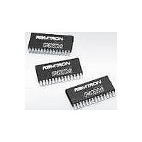
FM1808-70-S Ramtron, FM1808-70-S Datasheet

FM1808-70-S
Specifications of FM1808-70-S
Available stocks
Related parts for FM1808-70-S
FM1808-70-S Summary of contents
Page 1
... DQ0 12 17 DQ1 DQ2 13 16 VSS 14 15 Ordering Information FM1808-70- access, 28-pin “Green” DIP FM1808-70- access, 28-pin “Green” SOIC Ramtron International Corporation 1850 Ramtron Drive, Colorado Springs, CO 80921 (800) 545-FRAM, (719) 481-7000 http://www.ramtron.com VDD WE A13 A8 A9 A11 OE A10 ...
Page 2
... Address changes that occur after /CE goes low will be ignored until the next falling edge occurs. /OE Input Output Enable: Asserting /OE low causes the FM1808 to drive the data bus when valid data is available. Deasserting /OE high causes the DQ pins to be tri-stated. /WE Input Write Enable: Asserting /WE low causes the FM1808 to write the contents of the data bus to the address location latched by the falling edge of /CE ...
Page 3
... In a /CE controlled write, the /WE signal is asserted prior to beginning the memory cycle. That is, /WE is low when /CE falls. In this case, the part begins the memory cycle as a write. The FM1808 will not drive the data bus regardless of the state of /OE /WE controlled write, the memory cycle begins on the falling edge of /CE ...
Page 4
... The memory architecture is based on an array of rows and columns. Each read or write access causes an endurance cycle for an entire row. In the FM1808, a row is 32 bits wide. Every 4-byte boundary marks the beginning of a new row. Endurance can be optimized by ensuring frequently accessed data is located in different rows ...
Page 5
... MCU/MPU pin tri-states during the reset condition. The pullup resistor value should be chosen to ensure the /CE pin tracks V enough value that the current drawn when /CE is low is not an issue. level. DD MCU/ MPU It is Figure 3. Use of Pullup Resistor on /CE DD FM1808 yet a high FM1808 A(14:0) DQ Page ...
Page 6
... Std JESD22-A115-A) = 4.5V to 5.5V unless otherwise specified) DD Min Typ 4.5 5 2.0 -0.3 = -2.0 mA) 2 -4.2 mA) - Min Units 45 years FM1808 Ratings -1.0V to +7.0V -1.0V to +7.0V and V < V +1. -55° 125°C 300° C 4kV 300V 1 MSL-1 (-SG) 2 MSL-2 (-SG) Max Units Notes 5 ...
Page 7
... V (min) to First Access Start Last Access Complete Rev. 3.5 Nov. 2010 = 4.5V to 5.5V unless otherwise specified) DD Min 130 = 4.5V to 5.5V unless otherwise specified) DD Min 130 = 4.5V to 5.5V unless otherwise specified) DD Min Max 1 - (min FM1808 -70 Units Notes Max 2,000 -70 Units Notes ...
Page 8
... AC Test Conditions Input Pulse Levels Input rise and fall times Input and output timing levels Read Cycle Timing CE A0-14 OE DQ0-7 Write Cycle Timing - /CE Controlled Timing CE A0- DQ0-7 Rev. 3.5 Nov. 2010 = 5V) DD Min Max - Equivalent AC Load Circuit 1. FM1808 Units Notes OHZ Page ...
Page 9
... Write Cycle Timing - /WE Controlled Timing CE A0- DQ0-7 out DQ0-7 in Power Cycle Timing (min) IH (min) IH (min Rev. 3.5 Nov. 2010 (min) DD (min) DD (min (min) IH (min) IH (min) FM1808 (min) DD (min) DD (min (max) IL (max) IL (max) Page ...
Page 10
... XXXX= part number, S=speed (-70), P= package type (-PG, -SG) R=rev code, YY=year, WW=work week, LLLLLL= lot code B die rev., Year 2006, Work Week 30, Lot code 50013G RAMTRON FM1808-70-SG B063050013G FM1808 0.25 0.75 ° 0. ...
Page 11
... BSC 0.005 min. DIP Package Marking Scheme Legend: RAMTRON XXXXXXX-S-P RYYWWLLLLLLL Example: FM1808, 70ns speed, “Green”/RoHS DIP package, Rev. 3.5 Nov. 2010 1.380 1.565 0.014 0.022 XXXX= part number, S=speed (-70), P= package type (-PG, -SG) R=rev code, YY=year, WW=work week, LLLLLL= lot code B die rev ...
Page 12
... Added recommendation on CE pin during power cycles. 3.2 5/15/2007 Redraw package outlines, added marking scheme. 3.3 8/6/2007 Extended endurance to 10 3.4 12/18/2007 Updated MSL ratings. 3.5 11/22/2010 Not Recommended for New Designs. Alternative: FM18W08. Rev. 3.5 Nov. 2010 12 cycles based on recent test results. FM1808 Page ...


