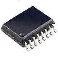
DG611DY Vishay, DG611DY Datasheet

DG611DY
Specifications of DG611DY
Available stocks
Related parts for DG611DY
DG611DY Summary of contents
Page 1
... To achieve such fast and clean switching performance, the DG611, DG612, DG613 are built on the Vishay Siliconix proprietary D/CMOS process. This process combines n-channel DMOS switching FETs with low-power CMOS control logic and drivers. An epitaxial layer prevents latchup. ...
Page 2
... Four SPST Switches per Package TRUTH TABLE Logic OFF 1 ON Logic “0” Logic “1” 4 V Part Number DG611DJ DG611DJ-E3 DG612DJ DG612DJ-E3 DG611DY DG611DY-E3 DG611DY-T1 DG611DY-T1-E3 DG612DY DG612DY-E3 DG612DY-T1 DG612DY-T1-E3 DG613DJ DG613DJ-E3 DG613DY DG613DY-E3 DG613DY-T1 DG613DY-T1-E3 Document Number: 70057 S11-0154-Rev. I, 31-Jan- OFF ...
Page 3
... RECOMMENDED OPERATING RANGE Parameter ANALOG Document Number: 70057 S11-0154-Rev. I, 31-Jan- mA, whichever occurs first or 20 mA, whichever occurs first or 20 mA, whichever occurs first DG611, DG612, DG613 Vishay Siliconix Limit Unit - (V-) - 0 ± ± 100 - 65 to 150 ° 125 470 600 mW 900 ...
Page 4
... DG611, DG612, DG613 Vishay Siliconix a SPECIFICATIONS Parameter Symbol Analog Switch e Analog Signal Range V ANALOG Switch On-Resistance R DS(on) R Resistance Match Bet Ch. Source Off Leakage I S(off) Drain Off Leakage Current I D(off) Switch On Leakage Current I D(on) Digital Control Input Voltage High V Input Voltage Low ...
Page 5
... Document Number: 70057 S11-0154-Rev. I, 31-Jan-11 a Test Conditions Unless Otherwise Specified Temp Full mA Room 300 Room Room See test circuit, figure DG611, DG612, DG613 Vishay Siliconix A Suffix D Suffix - 55 °C to 125 ° ° ° Ty.p Min. Max. Min S(of f), D( D(on ...
Page 6
... DG611, DG612, DG613 Vishay Siliconix TYPICAL CHARACTERISTICS (25 °C, unless otherwise noted Logic Supply Voltage (V) L Input Switching Threshold vs. V 400 350 300 250 200 150 25 °C 100 125 ° Drain Voltage ( vs. V and Temperature DS(on 100 pA I D(on 0 Temperature (°C) Leakage Currents vs. Temperature www ...
Page 7
... 300 GND V- V- Document Number: 70057 S11-0154-Rev. I, 31-Jan-11 Crosstalk - 100 Level Driver Translator Figure Logic Input ± Switch Output L Figure 2. Switching Time DG611, DG612, DG613 Vishay Siliconix 100K 100K Frequency (Hz) Supply Currents vs. Switching Frequency S D DMOS Switch OFF C (includes fixture and stray capacitance) ...
Page 8
... DG611, DG612, DG613 Vishay Siliconix TEST CIRCUITS + GND - 3 V Figure 3. Charge Injection APPLICATIONS High-Speed Sample-and-Hold In a fast sample-and-hold application, the analog switch characteristics are critical. A fast switch reduces aperture uncertainty. A low charge injection eliminates offset (step) errors. A low leakage reduces droop errors. The CLC111, a fast input buffer, helps to shorten acquisition and settling times ...
Page 9
... Figure 7. A High-Speed GaAs FET Driver that Saves Power Vishay Siliconix maintains worldwide manufacturing capability. Products may be manufactured at one of several qualified locations. Reliability data for Silicon Technology and Package Reliability represent a composite of all qualified locations. For related documents such as package/tape drawings, part marking, and reliability data, see www ...
Page 10
... Vishay product could result in personal injury or death. Customers using or selling Vishay products not expressly indicated for use in such applications their own risk and agree to fully indemnify and hold Vishay and its distributors harmless from and against any and all claims, liabilities, expenses and damages arising or resulting in connection with such use or sale, including attorneys fees, even if such claim alleges that Vishay or its distributor was negligent regarding the design or manufacture of the part ...


