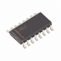
MAX4566CSE Maxim Integrated Products, MAX4566CSE Datasheet

MAX4566CSE
Specifications of MAX4566CSE
Available stocks
Related parts for MAX4566CSE
MAX4566CSE Summary of contents
Page 1
... SWITCHES SHOWN 1 ON FOR LOGIC “0” INPUT Rail-to-Rail is a registered trademark of Nippon Motorola Ltd. ________________________________________________________________ Maxim Integrated Products For free samples & the latest literature: http://www.maxim-ic.com, or phone 1-800-998-8800. For small orders, phone 408-737-7600 ext. 3468. Quad/Dual, Low-Voltage, Bidirectional RF/Video Switches ____________________________Features High 50Ω ...
Page 2
Quad/Dual, Low-Voltage, Bidirectional RF/Video Switches ABSOLUTE MAXIMUM RATINGS (Voltages Referenced to GND) V+ ...........................................................................-0.3V, +13.0V V- ............................................................................-13.0V, +0. V-...................................................................-0.3V, +13.0V All Other Pins (Note 1) ..........................(V- - 0.3V) to (V+ + 0.3V) Continuous Current into Any Terminal..............................±25mA Peak ...
Page 3
ELECTRICAL CHARACTERISTICS—Dual Supplies (continued) (V+ = +4.5V to +5.5V -4.5V to -5.5V, V values are +25°C.) A PARAMETER SYMBOL SWITCH DYNAMIC CHARACTERISTICS Turn-On Time Turn-Off Time Break-Before-Make Time Delay (MAX4566/MAX4567 only) Charge Injection (Note 3) ...
Page 4
Quad/Dual, Low-Voltage, Bidirectional RF/Video Switches ELECTRICAL CHARACTERISTICS—Single +5V Supply (V+ = +4.5V to +5.5V 0V 0.8V, V INL +25°C.) A PARAMETER SYMBOL ANALOG SWITCH V COM_ Analog Signal Range V NO_ Signal-Path On-Resistance ...
Page 5
ELECTRICAL CHARACTERISTICS—Single +3V Supply (V+ = +2.7V to +3.6V 0V 0.8V, V INL +25°C.) A PARAMETER SYMBOL ANALOG SWITCH V Analog Signal Range V NO_ Signal-Path On-Resistance LOGIC INPUT IN_ Input Logic Threshold ...
Page 6
Quad/Dual, Low-Voltage, Bidirectional RF/Video Switches __________________________________________Typical Operating Characteristics (V+ = +5V -5V +25°C, GND = 0V, packages are surface mount, unless otherwise noted RESISTANCE vs. V COM (DUAL SUPPLIES) 1000 V+ = 1.2V, V- ...
Page 7
Operating Characteristics (continued) (V+ = +5V -5V +25°C, GND = 0V, packages are surface mount, unless otherwise noted.) A LOGIC-LEVEL THRESHOLD VOLTAGE vs. V+ SUPPLY VOLTAGE 3.0 2.5 2.0 1.5 1.0 0 ...
Page 8
Quad/Dual, Low-Voltage, Bidirectional RF/Video Switches ______________________________________________________________Pin Description PIN MAX4565 MAX4566 MAX4567 1, 10 12 ...
Page 9
GND_. The four on MOSFETs also have capacitance to ground that, together with the series resistance, forms a lowpass fil- ter. All of these capacitances are distributed evenly along the series resistance, so they act as ...
Page 10
Quad/Dual, Low-Voltage, Bidirectional RF/Video Switches Single-Supply Operation The MAX4565/MAX4566/MAX4567 operate from a sin- gle supply between +2.7V and +12V when V- is con- nected to GND. All of the bipolar precautions must be observed. Note, however, that these parts are ...
Page 11
The MAX4567 has two V+ and two V- pins. Make DC connections to only one of each to minimize crosstalk. Do not route DC current into one of the pins and out the other ...
Page 12
Quad/Dual, Low-Voltage, Bidirectional RF/Video Switches With its excellent off isolation, the MAX4565 is ideal for use in high-frequency video multiplexers. Figure 2 shows such an application for switching any one of four video inputs to a single output. The same ...
Page 13
Circuits/Timing Diagrams (continued) 10nF +5V V+ MAX4566 V IN_ IN_ GND_ 50 10nF * REPEAT TEST FOR OTHER PAIR OF SWITCHES. 10nF +5V V+ MAX4567 V IN_ IN_ GND_ 50 10nF ** REPEAT TEST FOR OTHER SWITCH. Figure 4. ...
Page 14
Quad/Dual, Low-Voltage, Bidirectional RF/Video Switches _________________________________Test Circuits/Timing Diagrams (continued) 10nF +5V V+ NO_ OR NC_ MAX4565 MAX4566 MAX4567 V IN_ IN_ COM_ GND_ V- 50 10nF - CONNECTED TO GND (0V) FOR SINGLE-SUPPLY OPERATION. Figure 5. Charge Injection ...
Page 15
Test Circuits/Timing ______________Diagrams (continued) 10nF + IN_ NO_ NC_ MAX4565 MAX4566 MAX4567 COM_ GND_ V- 10nF -5V ALL GND_ PINS ARE CONNECTED TO GROUND PLANE (0V). Figure 7. NO_, NC_, COM_ Capacitance MAX4566 COM1 IN1 IN2 ...
Page 16
... MAX4565C/D 0°C to +70°C MAX4565EPP -40°C to +85°C MAX4565EWP -40°C to +85°C MAX4565EAP -40°C to +85°C MAX4566CPE 0°C to +70°C MAX4566CSE 0°C to +70°C MAX4566CEE 0°C to +70°C MAX4566C/D 0°C to +70°C MAX4566EPE -40°C to +85°C MAX4566ESE -40°C to +85°C ________________________________________________________Package Information Maxim cannot assume responsibility for use of any circuitry other than circuitry entirely embodied in a Maxim product ...


