MAX4889BETO+T Maxim Integrated Products, MAX4889BETO+T Datasheet - Page 9
MAX4889BETO+T
Manufacturer Part Number
MAX4889BETO+T
Description
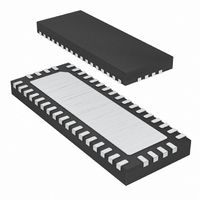
IC SWITCH OCTAL SPDT 42TQFN
Manufacturer
Maxim Integrated Products
Datasheet
1.MAX4889BETO.pdf
(12 pages)
Specifications of MAX4889BETO+T
Function
Switch
Circuit
8 x SPDT
On-state Resistance
7 Ohm
Voltage Supply Source
Single Supply
Voltage - Supply, Single/dual (±)
1.65 V ~ 3.6 V
Operating Temperature
-40°C ~ 85°C
Mounting Type
Surface Mount
Package / Case
42-WFQFN Exposed Pad
Lead Free Status / RoHS Status
Lead free / RoHS Compliant


The MAX4889B high-speed passive switch routes PCI
Express (PCIe) data or other high-speed signals with
amplitude of ≤ 1.2V
voltage close to 0V between two possible destinations.
The MAX4889B is ideal for routing PCIe signals to
change system configuration. For example, in a graphics
application, four MAX4889B devices create two sets of
eight lanes from a single 16-lane bus. The MAX4889C
feature a 10µA (typ) source current and a 60kΩ (typ)
internal biasing resistor to GND at the _OUT_ terminals.
The MAX4889C is ideal for dual capacitively coupled
applications such as SAS and SATA. The MAX4889B/
MAX4889C feature a single digital control input (SEL) to
switch signal paths. SEL has a 70kΩ (typ) pulldown
resistor to GND.
The MAX4889B/MAX4889C are fully specified to oper-
ate from a single 3.0V to 3.6V power supply.
The MAX4889B/MAX4889C provide a single digital
control input (SEL) to select the signal path between
the _IN_ and _OUT_ channels. The truth tables for the
MAX4889B/MAX4889C are illustrated in the Functional
Diagram/Truth Table . SEL has a 70kΩ (typ) pulldown
resistor to GND.
The MAX4889B/MAX4889C accept standard PCIe signals
to a maximum of (V
nels are routed to either the _OUTA+ or _OUTB+ chan-
nels. Signals on the _IN- channels are routed to either the
_OUTA- or _OUTB- channels. The MAX4889B/MAX4889C
are bidirectional switches, allowing _IN_ and _OUT_ to be
used as either inputs or outputs.
_______________________________________________________________________________________
CC
P-P
2.5/5.0/8.0Gbps PCIe Passive Switches
Digital Control Input (SEL)
Detailed Description
- 1.8V). Signals on the _IN+ chan-
differential, and common-mode
Analog Signal Levels
The MAX4889B/MAX4889C primary applications are
aimed at reallocating PCIe lanes (see the Typical
Operating Circuit: Video Graphics Cards ). For example,
in graphics applications, several manufacturers have
found that it is possible to improve performance by a fac-
tor of nearly two by splitting a single 16-lane PCIe bus
into two 8-lane buses. Two of the more prominent exam-
ples are SLI (Scaled Link Interface) and CrossFire. Four
MAX4889Bs permit a computer motherboard to operate
properly with a single 16-lane graphics card, which can
later be upgraded to dual cards.
High-speed switches require proper layout and design
procedures for optimum performance. Keep controlled-
impedance PCB traces as short as possible or follow
impedance layouts per the PCIe specification. Ensure
that power-supply bypass capacitors are placed as
close as possible to the device. Multiple bypass capac-
itors are recommended. Connect all grounds and the
exposed pad to large ground planes.
Applications Information
PCIe Switching
Board Layout
9
Related parts for MAX4889BETO+T
Image
Part Number
Description
Manufacturer
Datasheet
Request
R

Part Number:
Description:
MAX7528KCWPMaxim Integrated Products [CMOS Dual 8-Bit Buffered Multiplying DACs]
Manufacturer:
Maxim Integrated Products
Datasheet:
Part Number:
Description:
Single +5V, fully integrated, 1.25Gbps laser diode driver.
Manufacturer:
Maxim Integrated Products
Datasheet:
Part Number:
Description:
Single +5V, fully integrated, 155Mbps laser diode driver.
Manufacturer:
Maxim Integrated Products
Datasheet:
Part Number:
Description:
VRD11/VRD10, K8 Rev F 2/3/4-Phase PWM Controllers with Integrated Dual MOSFET Drivers
Manufacturer:
Maxim Integrated Products
Datasheet:
Part Number:
Description:
Highly Integrated Level 2 SMBus Battery Chargers
Manufacturer:
Maxim Integrated Products
Datasheet:
Part Number:
Description:
Current Monitor and Accumulator with Integrated Sense Resistor; ; Temperature Range: -40°C to +85°C
Manufacturer:
Maxim Integrated Products
Part Number:
Description:
TSSOP 14/A�/RS-485 Transceivers with Integrated 100O/120O Termination Resis
Manufacturer:
Maxim Integrated Products
Part Number:
Description:
TSSOP 14/A�/RS-485 Transceivers with Integrated 100O/120O Termination Resis
Manufacturer:
Maxim Integrated Products
Part Number:
Description:
QFN 16/A�/AC-DC and DC-DC Peak-Current-Mode Converters with Integrated Step
Manufacturer:
Maxim Integrated Products
Part Number:
Description:
TDFN/A/65V, 1A, 600KHZ, SYNCHRONOUS STEP-DOWN REGULATOR WITH INTEGRATED SWI
Manufacturer:
Maxim Integrated Products
Part Number:
Description:
Integrated Temperature Controller f
Manufacturer:
Maxim Integrated Products
Part Number:
Description:
SOT23-6/I�/45MHz to 650MHz, Integrated IF VCOs with Differential Output
Manufacturer:
Maxim Integrated Products
Part Number:
Description:
SOT23-6/I�/45MHz to 650MHz, Integrated IF VCOs with Differential Output
Manufacturer:
Maxim Integrated Products
Part Number:
Description:
EVALUATION KIT/2.4GHZ TO 2.5GHZ 802.11G/B RF TRANSCEIVER WITH INTEGRATED PA
Manufacturer:
Maxim Integrated Products
Part Number:
Description:
QFN/E/DUAL PCIE/SATA HIGH SPEED SWITCH WITH INTEGRATED BIAS RESISTOR
Manufacturer:
Maxim Integrated Products
Datasheet: