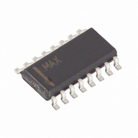
MAX4559CSE+ Maxim Integrated Products, MAX4559CSE+ Datasheet - Page 10

MAX4559CSE+
Manufacturer Part Number
MAX4559CSE+
Description
IC MULTIPLEXER DUAL 4X1 16SOIC
Manufacturer
Maxim Integrated Products
Datasheet
1.MAX4558ESE.pdf
(16 pages)
Specifications of MAX4559CSE+
Function
Multiplexer
Circuit
2 x 4:1
On-state Resistance
160 Ohm
Voltage Supply Source
Single, Dual Supply
Voltage - Supply, Single/dual (±)
5V, ±2.5V, ±3.3V
Current - Supply
1µA
Operating Temperature
0°C ~ 70°C
Mounting Type
Surface Mount
Package / Case
16-SOIC (0.154", 3.90mm Width)
Lead Free Status / RoHS Status
Lead free / RoHS Compliant
ESD performance depends on several conditions.
Contact Maxim for a reliability report that documents
test setup, methodology, and results.
Figure 6 shows the Human Body Model, and Figure 7
shows the current waveform it generates when dis-
charged into a low impedance. This model consists of
a 100pF capacitor charged to the ESD voltage of inter-
est, which is then discharged into the test device
through a 1.5kΩ resistor.
The MAX4558/MAX4559/MAX4560 are typical of most
CMOS analog switches. They have three supply pins:
V
CMOS switches and set the limits of the analog voltage
on every switch. Internal reverse ESD-protection diodes
connect between each analog signal pin and both V
and V
of these diodes conducts. The only currents drawn
from V
age currents of these ESD diodes.
Although the ESD diodes on a given signal pin are
identical and therefore fairly well balanced, they are
reverse biased differently. Each is biased by either V
or V
vary as the signal varies. The difference in the two
diode leakages to the V
analog signal-path leakage current. All analog leakage
current flows between each input and one of the supply
±15kV ESD-Protected, Low-Voltage, CMOS
Analog Multiplexers/Switches
10
CC
, V
EE
______________________________________________________________________________________
EE
CC
EE
and the analog signal. Their leakage currents
. If any analog signal exceeds V
, and GND. V
or V
EE
Power-Supply Considerations
during normal operation are the leak-
CC
CC
and V
and V
ESD Test Conditions
Human Body Model
EE
EE
pins constitutes the
drive the internal
CC
or V
EE
, one
CC
CC
terminals, not to the other switch terminal. This is why
both sides of a given switch can show leakage currents
of either the same or opposite polarity.
V
translators, and set the input logic limits. The logic-level
translators convert the logic levels into switched V
and V
This drive signal is the only connection between the
logic supplies and logic signals and the analog sup-
plies. V
GND.
The logic-level thresholds are TTL/CMOS compatible
when V
slightly. When V
about 3.1V (above the TTL-guaranteed high-level mini-
mum of 2.4V, but still compatible with CMOS outputs).
In 50Ω systems, signal response is reasonably flat up
to 50MHz (see Typical Operating Characteristics ).
Above 20MHz, the on response has several minor
peaks that are highly layout dependent. The problem is
not turning the switch on, but turning it off. The off-state
switch acts like a capacitor and passes higher frequen-
cies with less attenuation. At 1MHz, off-isolation is
about -68dB in 50Ω systems, becoming worse (approx-
imately 20dB per decade) as the frequency increases.
Higher circuit impedance also degrades off-isolation.
Adjacent channel attenuation is about 3dB above that
of a bare IC socket and is entirely due to capacitive
coupling.
CC
and GND power the internal logic and logic-level
EE
CC
CC
signals to drive the gates of the analog switch.
is +5V. As V
and V
CC
High-Frequency Performance
EE
reaches +12V, the threshold is
have ESD-protection diodes to
CC
rises, the threshold increases
CC


