ADG512BR Analog Devices Inc, ADG512BR Datasheet
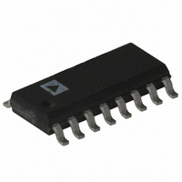
IC SWITCH QUAD SPST 16SOIC

ADG512BR

Manufacturer Part Number
ADG512BR
Description
IC SWITCH QUAD SPST 16SOIC
Manufacturer
Analog Devices Inc
Series
LC²MOSr
Type
Analog Switchr
Datasheet

Specifications of ADG512BR

Rohs Status
RoHS non-compliant
Function
Switch
Circuit
4 x SPST - NC
On-state Resistance
30 Ohm
Voltage Supply Source
Single, Dual Supply
Voltage - Supply, Single/dual (±)
3V, ±5V
Current - Supply
0.0001µA
Operating Temperature
-40°C ~ 85°C
Mounting Type
Surface Mount
Package / Case
16-SOIC (0.154", 3.90mm Width)
Multiplexer Configuration
Quad SPST
Number Of Inputs
4
Number Of Outputs
4
Number Of Channels
4
Analog Switch On Resistance
200@3VOhm
Analog Switch Turn On Time
600ns
Analog Switch Turn Off Time
120ns
Package Type
SOIC N
Power Supply Requirement
Single/Dual
Single Supply Voltage (min)
4.5V
Single Supply Voltage (typ)
5V
Single Supply Voltage (max)
5.5V
Dual Supply Voltage (min)
±4.5V
Dual Supply Voltage (typ)
±5V
Dual Supply Voltage (max)
±5.5V
Power Dissipation
600mW
Supply Current
0.001mA
Mounting
Surface Mount
Pin Count
16
Operating Temp Range
-40C to 85C
Operating Temperature Classification
Industrial
Lead Free Status / RoHS Status
Not Compliant

Available stocks

Company
Part Number
Manufacturer
Quantity
Price
Part Number:
ADG512BR
Manufacturer:
AD
Quantity:
5 510
Part Number:
ADG512BR
Manufacturer:
ADI/亚德诺
Quantity:
20 000
Part Number:
ADG512BRZ
Manufacturer:
AD
Quantity:
3 000
Part Number:
ADG512BRZ
Manufacturer:
ADI/亚德诺
Quantity:
20 000
Part Number:
ADG512BRZ
Quantity:
41
a
GENERAL DESCRIPTION
The ADG511, ADG512 and ADG513 are monolithic CMOS
ICs containing four independently selectable analog switches.
These switches feature low, well-controlled on resistance and
wide analog signal range, making them ideal for precision
analog signal switching.
These switch arrays are fabricated using Analog Devices’
advanced linear compatible CMOS (LC
offers the additional benefits of low leakage currents, ultralow
power dissipation and low capacitance for fast switching speeds
with minimum charge injection. These features make the
ADG511, ADG512 and ADG513 the optimum choice for a
wide variety of signal switching tasks in precision analog signal
processing and data acquisition systems.
The ability to operate from single +3 V, +5 V or ± 5 V bipolar
supplies make the ADG511, ADG512 and ADG513 perfect for
use in battery-operated instruments, 4–20 mA loop systems and
with the new generation of DACs and ADCs from Analog
Devices. The use of 5 V supplies and reduced operating currents
give much lower power dissipation than devices operating from
± 15 V supplies.
2
MOS) process which
Precision 5 V/3 V Quad SPST Switches
The ADG511, ADG512 and ADG513 contain four indepen-
dent SPST switches. The ADG511 and ADG512 differ only in
that the digital control logic is inverted. The ADG511 switch is
turned on with a logic low on the appropriate control input,
while a logic high is required for the ADG512. The ADG513
contains two switches whose digital control logic is similar to
that of the ADG511 while the logic is inverted in the remaining
two switches.
PRODUCT HIGHLIGHTS
1. 5 Volt Single Supply Operation
2. Ultralow Power Dissipation
3. Low R
4. Break-Before-Make Switching
IN2
IN3
IN4
IN1
The ADG511/ADG512/ADG513 offers high performance,
including low on resistance and wide signal range, fully
specified and guaranteed with +3 V, ± 5 V as well as +5 V
supply rails.
CMOS construction ensures ultralow power dissipation.
Switches are guaranteed to have break-before-make opera-
tion. This allows multiple outputs to be tied together for
multiplexer applications without the possibility of momentary
shorting between channels.
ADG511
ADG511/ADG512/ADG513
ON
FUNCTIONAL BLOCK DIAGRAMS
SWITCHES SHOWN FOR A LOGIC "1" INPUT
S1
D1
S2
D2
S3
D3
S4
D4
IN2
IN3
IN4
IN1
ADG512
S1
D1
S2
D2
S3
D3
S4
D4
IN2
IN3
IN4
IN1
LC
ADG513
2
MOS
S1
D1
S2
D2
S3
D3
S4
D4

Related parts for ADG512BR

ADG512BR Summary of contents

Page 1

GENERAL DESCRIPTION The ADG511, ADG512 and ADG513 are monolithic CMOS ICs containing four independently selectable analog switches. These switches feature low, well-controlled on resistance and wide analog signal range, making them ideal for precision analog signal switching. These switch ...

Page 2

ADG511/ADG512/ADG513–SPECIFICATIONS Dual Supply ( 10 Parameter 25 C ANALOG SWITCH Analog Signal Range LEAKAGE CURRENTS ± 0.025 Source OFF Leakage I (OFF) S ± 0.1 ± 0.025 Drain OFF Leakage I (OFF) ...

Page 3

Single Supply ( 10 Parameter 25 C ANALOG SWITCH Analog Signal Range LEAKAGE CURRENTS ± 0.025 Source OFF Leakage I (OFF) S ± 0.1 ± 0.025 Drain OFF Leakage I (OFF) D ...

Page 4

ADG511/ADG512/ADG513–SPECIFICATIONS Single Supply (V = 3 Parameter ANALOG SWITCH Analog Signal Range R ON LEAKAGE CURRENTS Source OFF Leakage I (OFF) S Drain OFF Leakage I (OFF) D Channel ON Leakage (ON) D ...

Page 5

... Therefore, proper ESD precautions are recommended to avoid performance degradation or loss of functionality. 1 Model ADG511BN ADG511BR ADG511ABR ADG511TQ ADG512BN ADG512BR ADG512ABR ADG513BN ADG513BR ADG513ABR NOTES 1 For availability of MIL-STD-883, Class B processed parts, contact factory. 2 3.3 V specifications apply over 0°C to 70°C temperature range. ...

Page 6

ADG511/ADG512/ADG513 PIN CONFIGURATION (DIP/SOIC) IN1 ADG511 ADG512 ADG513 TOP VIEW GND 5 12 (Not to Scale IN4 ...

Page 7

Typical Performance Characteristics–ADG511/ADG512/ADG513 + – + – –5 –4 –3 –2 – ...

Page 8

ADG511/ADG512/ADG513 0.006 – (ON) 0.004 + 0.002 0.000 –0.002 –0.004 –0.006 –5 –4 –3 –2 – – DRAIN OR SOURCE VOLTAGE – ...

Page 9

Test Circuits V1 0 GND IN1, IN2 V GND 0.1 ...

Page 10

ADG511/ADG512/ADG513 GND SS 0 OUT V IN1 OUT 0 ...

Page 11

OUTLINE DIMENSIONS Dimensions shown in inches and (mm). 16-Lead Plastic DIP (N-16) 0.840 (21.34) 0.745 (18.92 0.280 (7.11) 0.240 (6.10 PIN 1 0.060 (1.52) 0.015 (0.38) 0.210 (5.33) MAX 0.130 (3.30) 0.160 (4.06) MIN 0.115 (2.93) ...

Page 12

ADG511/ADG512/ADG513–Revision History Location Data Sheet changed from REV REV. C. Changes to Specifications table, Dual Supply, and Notes: “T Versions” made singular . . . . . . . . . . . . . . . . ...

Related keywords