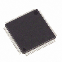
DS21554LB+ Maxim Integrated Products, DS21554LB+ Datasheet - Page 96

DS21554LB+
Manufacturer Part Number
DS21554LB+
Description
IC TXRX E1 5V 100-LQFP
Manufacturer
Maxim Integrated Products
Datasheet
1.DS2154LNA2.pdf
(124 pages)
Specifications of DS21554LB+
Function
Single-Chip Transceiver
Interface
E1, HDLC, J1, T1
Number Of Circuits
1
Voltage - Supply
4.75 V ~ 5.25 V
Current - Supply
75mA
Operating Temperature
0°C ~ 70°C
Mounting Type
Surface Mount
Package / Case
100-LQFP
Includes
Remote and AIS Alarm Detector / Generator
Product
Framer
Number Of Transceivers
1
Data Rate
1.544 Mbps
Supply Voltage (max)
5.25 V
Supply Voltage (min)
4.75 V
Supply Current (max)
75 mA (Typ)
Maximum Operating Temperature
+ 70 C
Minimum Operating Temperature
0 C
Mounting Style
SMD/SMT
Ic Interface Type
Parallel, Serial
Supply Voltage Range
4.75V To 5.25V
Operating Temperature Range
0°C To +70°C
Digital Ic Case Style
LQFP
No. Of Pins
100
Filter Terminals
SMD
Rohs Compliant
Yes
Lead Free Status / RoHS Status
Lead free / RoHS Compliant
Power (watts)
-
Lead Free Status / Rohs Status
Lead free / RoHS Compliant
rising edge of JTCLK following entry into the Capture-DR state. Shift-DR can be used to shift the
identification code out serially via JTDO. During Test-Logic-Reset, the identification code is forced into
the instruction register’s parallel output. The ID code will always have a one in the LSB position. The
next 11 bits identify the manufacturer’s JEDEC number and number of continuation bytes followed by 16
bits for the device and 4 bits for the version. See
SCT devices.
Table 16-2. ID Code Structure
MSB
Version
Contact Factory
4 bits
Table 16-3. Device ID Codes
16.2.
IEEE 1149.1 requires a minimum of two test registers; the bypass register and the boundary scan register.
An optional test register has been included with the DS21354/554 design. This test register is the
identification register and is used in conjunction with the IDCODE instruction and the Test-Logic-Reset
state of the TAP controller.
Boundary Scan Register
This register contains both a shift register path and a latched parallel output for all control cells and
digital I/O cells and is n bits in length. See
Bypass Register
This is a single one-bit shift register used in conjunction with the BYPASS, CLAMP, and HIGHZ
instructions that provides a short path between JTDI and JTDO.
Identification Register
The identification register contains a 32-bit shift register and a 32-bit latched parallel output. This register
is selected during the IDCODE instruction and when the TAP controller is in the Test-Logic-Reset state.
See
Table 16-3
Test Registers
DEVICE
DS21354
DS21554
DS21352
DS21552
and
Table 16-4
for more information on bit usage.
Device ID
16 bits
16-BIT ID
0005h
0003h
0004h
0002h
Table 16-4
96 of 124
Table
for all the cell bit locations and definitions.
16-2.
00010100001
JEDEC
Table 16-3
lists the device ID codes for the
LSB
1
1


