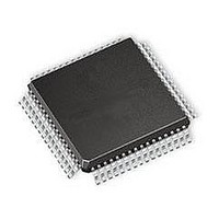
SI3220-KQ Silicon Laboratories Inc, SI3220-KQ Datasheet - Page 32

SI3220-KQ
Manufacturer Part Number
SI3220-KQ
Description
IC SLIC/CODEC DUAL-CH 64TQFP
Manufacturer
Silicon Laboratories Inc
Series
ProSLIC®r
Specifications of SI3220-KQ
Package / Case
*
Function
Subscriber Line Interface Concept (SLIC), CODEC
Interface
GCI, PCM, SPI
Number Of Circuits
2
Voltage - Supply
3.3V, 5V
Current - Supply
65mA
Power (watts)
941mW
Operating Temperature
0°C ~ 70°C
Mounting Type
Surface Mount
Includes
Battery Switching, BORSCHT Functions, DTMF Generation and Decoding, FSK Tone Generation, Modem and Fax Tone Detection
Product
Telecom
Supply Voltage (min)
3.13 V
Supply Current
22 mA
Maximum Operating Temperature
+ 70 C
Minimum Operating Temperature
0 C
Mounting Style
SMD/SMT
Number Of Channels
2
Lead Free Status / RoHS Status
Contains lead / RoHS non-compliant
Available stocks
Company
Part Number
Manufacturer
Quantity
Price
Company:
Part Number:
SI3220-KQ
Manufacturer:
SILICON
Quantity:
14 000
Company:
Part Number:
SI3220-KQ
Manufacturer:
Silicon Laboratories Inc
Quantity:
10 000
Part Number:
SI3220-KQ
Manufacturer:
SI
Quantity:
20 000
Company:
Part Number:
SI3220-KQR
Manufacturer:
SIPEX
Quantity:
10 000
Part Number:
SI3220-KQR
Manufacturer:
SILICON LABS/芯科
Quantity:
20 000
Si3220/Si3225
Only one calibration should be necessary if the system
remains powered up.
To optimize performance, it is recommended that the
user perform the following steps when running the CAL
routines:
1. Set CALR1 = 0x3F and CALR2 = 0x3E. This enables all
2. Set the CAL bit in the CALR1 register. This runs the first
3. Set the ProSLIC to the ACTIVE state (set
4. Set CALR2 = 0x01. This enables only the AC longitudinal
5. Set the CAL bit in the CALR1 register.
There is an initial settling period of approximately
300 ms that is required prior to running the first set of
calibration routines. Each calibration routine requires
approximately 1 ms to complete, except for the ac
longitudinal balance routine, which requires up to
100 ms. An additional 300 ms settling period is also
required after going to the ACTIVE state and prior to
running the ac longitudinal balance routine.
During calibration, V
32
Loop Voltage Sense
(V
TIP Voltage Sense
RING Voltage Sense
Loop Current Sense
Battery Voltage Sense
Longitudinal Current
Sense
External Ringing Genera-
tor Voltage Sense
External Ringing Genera-
tor Current Sense
*Note: I
calibration routines except the AC longitudinal balance
(CALCMBAL) routine.
set of calibration routines.
LINEFEED = 0x01)
balance calibration routine.
TIP
– V
approximately 500 µA.
Parameter
LOOP
RING
and I
)
LONG
Table 19. Register and RAM Locations Used for Loop Monitoring
TIP
are calculated values based on measured I
and V
Register/RAM
RING
Mnemonic
VRNGNG
IRNGNG
VLOOP
VRING
ILONG
ILOOP
VBAT
VTIP
are controlled by the
Preliminary Rev. 0.91
IRNGNG[15:0
VRNGNG[15:
VLOOP[15:0]
VRING[15:0]
ILONG[15:0]
ILOOP[15:0]
VBAT[15:0]
VTIP[15:0]
RAM Bits
Register/
0]
]
calibration engine to provide the correct external voltage
conditions for the algorithm. Calibration should always
be performed in the on-hook active state. The TIP and
RING leads must not be connected to ground during
calibration.
Loop Voltage and Current Monitoring
The Dual ProSLIC chipset continuously monitors the
TIP and RING voltages and currents. These values are
available in registers. An internal 8-bit A/D converter
samples the measured voltages and currents from the
analog sense circuitry and translates them into the
digital domain. The A/D updates the samples at an
800 Hz rate for all inputs except VRNGNG and
IRNGNG, which are sampled at 8 kHz to provide higher
resolution for zero crossing detection in external ringing
applications. Two derived values, the loop voltage
(V
For ground start operation, the values reported are
V
Table 19 lists the register set associated with the loop
monitoring functions.
The Dual ProSLIC chipsets also include the ability to
perform loop diagnostics functions as outlined in "Line
Test and Diagnostics" on page 85.
RING
TIP
Q1
– V
–I
64.07 to 160.173 V
64.07 to 160.173 V
64.07 to 160.173 V
and the current flowing in the RING lead.
Q4
0 to 101.09 mA
0 to 101.09 mA
Measurement
0 to 160.173 V
RING
0 to 64.07 V
0 to 64.07 V
0 to 64.07 V
662.83 mA
currents. The resulting effective resolution is
0 to 63.3 V
332.04 V
Range
) and the loop current also are reported.
10.172 mV
LSB Size
4.907 mV
4.907 mV
4.907 mV
4.907 mV
3.097 µ A
3.097 µ A
20.3 µ A
Resolution
Effective
500 µ A*
500 µ A*
251 mV
628 mV
251 mV
628 mV
251 mV
628 mV
251 mV
628 mV
1.302 V
2.6 mA


