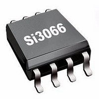
SI3066-B-FS Silicon Laboratories Inc, SI3066-B-FS Datasheet - Page 16

SI3066-B-FS
Manufacturer Part Number
SI3066-B-FS
Description
IC DAA ENH FCC LINE-SIDE 8SOIC
Manufacturer
Silicon Laboratories Inc
Type
Single Chipr
Datasheet
1.SI3066-B-FS.pdf
(40 pages)
Specifications of SI3066-B-FS
Package / Case
*
Function
Direct Access Arrangement (DAA)
Number Of Circuits
1
Current - Supply
9mA
Operating Temperature
0°C ~ 70°C
Mounting Type
Surface Mount
Includes
Billing Tone Detection, Line Voltage Monitor, Loop Current Monitor, Overload Detection, Ring Detector
Product
Modem Chip
Supply Voltage (min)
3 V
Maximum Operating Temperature
+ 70 C
Minimum Operating Temperature
0 C
Mounting Style
SMD/SMT
Lead Free Status / RoHS Status
Lead free / RoHS Compliant
Voltage - Supply
-
Power (watts)
-
Interface
-
Lead Free Status / RoHS Status
Lead free / RoHS Compliant, Lead free / RoHS Compliant
Available stocks
Company
Part Number
Manufacturer
Quantity
Price
Part Number:
SI3066-B-FS
Manufacturer:
SILICON LABS/芯科
Quantity:
20 000
Si3066
4.16.2. Type II Caller ID
Type II Caller ID sends the CID data while the phone is
off-hook and is often referred to as caller ID/call waiting
(CID/CW). To receive the CID data while off-hook, use
the following procedure:
1. The Caller Alert Signal (CAS) tone is sent from the
2. Since the DAA is the only device on the line and is
3. The CO then responds with the CID data, and the
4. The muting of the upstream data path by the
The CID data presented to the software could have up
to a 10% dc offset. The software caller ID decoder must
either use a high-pass or a band-pass filter to accurately
retrieve the caller ID data.
4.17. Gain Control
The Si3066 supports multiple receive gain and transmit
attenuation settings (Register 15). The receive path
supports gains of 0, 3, 6, 9, and 12 dB, as selected with
the ARX[2:0] bits. The receive path can be muted with
the RXM bit. The transmit path supports attenuations of
0, 3, 6, 9, and 12 dB, as selected with the ATX[2:0] bits.
The transmit path can be muted with the TXM bit.
4.18. Sample Rate Converter
The SRC [3:0] bits (Register 7, bits 3:0) are used to
select the sample rate. The following sample rates are
supported: 7200, 8000, 8229, 8400, 9000, 9600, 10286,
12000, 13714, and 16000 Hz.
4.19. Power Management
The Si3066 supports four basic power management
operation modes: normal operation, reset operation,
sleep mode, and full powerdown mode. The power
management modes are controlled by the PDL and
PDN bits (Register 6, bits [4:3]).
Upon powerup or following a reset, the Si3066 is in
reset operation. The PDL bit is set, and the PDN bit is
cleared. The system-side module is fully operational
16
Central Office (CO) and is digitized along with the
line data. The software must detect the presence of
this tone.
Type II CID-compliant, the software must mute its
upstream data output to avoid propagation of its
reply tone and the subsequent CID data. After
muting its upstream data output, the software must
then return an acknowledgement (ACK) tone to the
CO to request the transmission of the CID data.
software unmutes the upstream data output and
continues with normal operation.
software mutes the handset in a telephone
application so the user cannot hear the
acknowledgement tone and CID data being sent.
Rev. 1.0
except for the isolated capacitor link. No communication
between the system side and Si3066 can occur during
reset operation. Register bits associated with the
Si3066 are not valid in this mode.
The most common mode of operation is normal
operation. The PDL and PDN bits are cleared, and the
capacitive link is passing information between the
system side and the Si3066. A valid sample rate must
be programmed before entering this mode.
The Si3066 supports a low-power sleep mode for the
wake-up-on-ring feature of many modems. The sample
rate must be programmed with a valid non-zero value
before enabling sleep mode. The PDN bit must then be
set; the PDL bit cleared. To take the DAA out of sleep
mode, pulse (RESET) low.
In summary, the powerdown sequence for sleep mode
is as follows:
1. SRC[3:0] must have a valid non-zero value.
2. Set the PDN bit (Register 6, bit 3) and clear the PDL
The power-up sequence is as follows:
1. Reset the DAA by pulsing the RESET pin.
2. Program registers to required settings.
The Si3066 also supports an additional powerdown
mode. When the PDN and PDL bits are set, the DAA
enters a complete powerdown mode and draws
negligible current (deep sleep mode). Normal operation
is restored using the same process for taking the DAA
out of sleep mode.
4.20. Calibration
The Si3066 initiates an auto-calibration by default when
the device goes off-hook or experiences a loss in line
power. Calibration removes offsets that are present in
the on-chip ADC and could affect the ADC dynamic
range. Auto-calibration is initiated after the DAA dc
termination stabilizes and takes 273 ms to complete.
4.21. Revision Identification
The revision of the system-side module and line-side
(Si3066) can be determined using the REVA[3:0] bits
(Register 11, bits 3:0) and REVB[3:0] bits (Register 13,
bits 5:2), respectively. Table 9 lists the revision values.
bit (Register 6, bit 4).
Si3066 Revision
Table 9. Si3066 Revision Levels
A
B
Si3066 REVB[3:0]
1000
1001


