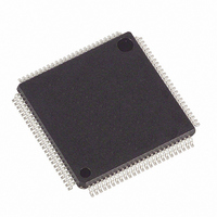
DS21354LN Maxim Integrated Products, DS21354LN Datasheet - Page 20

DS21354LN
Manufacturer Part Number
DS21354LN
Description
IC TXRX E1 1-CHIP 3.3V 100-LQFP
Manufacturer
Maxim Integrated Products
Datasheet
1.DS2154LNA2.pdf
(124 pages)
Specifications of DS21354LN
Function
Single-Chip Transceiver
Interface
E1, HDLC
Number Of Circuits
1
Voltage - Supply
3.14 V ~ 3.47 V
Current - Supply
75mA
Operating Temperature
-40°C ~ 85°C
Mounting Type
Surface Mount
Package / Case
100-LQFP
Includes
Remote and AIS Alarm Detector / Generator
Lead Free Status / RoHS Status
Contains lead / RoHS non-compliant
Power (watts)
-
Available stocks
Company
Part Number
Manufacturer
Quantity
Price
Company:
Part Number:
DS21354LN+
Manufacturer:
Maxim
Quantity:
180
Company:
Part Number:
DS21354LN+
Manufacturer:
DALLAS
Quantity:
1 085
3.1.3.
Signal Name:
Signal Description:
Signal Type:
Active-low, open-drain output that flags host controller during conditions and change of conditions
defined in the Status Registers 1 and 2 and the HDLC Status Register.
Signal Name:
Signal Description:
Signal Type:
Selects the DS2154 mode when high or the DS21354/DS21554 mode when low. If high, the JTRST is
internally pulled low. If low, JTRST has normal JTAG functionality. This pin has a 10kW pullup resistor.
Signal Name:
Signal Description:
Signal Type:
Set high to tri-state all output and I/O pins (including the parallel control port). Set low for normal
operation. Useful in board-level testing.
Signal Name:
Signal Description:
Signal Type:
Set low to select nonmultiplexed bus operation. Set high to select multiplexed bus operation.
Signal Name:
Signal Description:
Signal Type:
In nonmultiplexed bus operation (MUX = 0), serves as the data bus. In multiplexed bus operation
(MUX = 1), serves as an 8-bit multiplexed address/data bus.
Signal Name:
Signal Description:
Signal Type:
In nonmultiplexed bus operation (MUX = 0), serves as the address bus. In multiplexed bus operation
(MUX = 1), these pins are not used and should be tied low.
Signal Name:
Signal Description:
Signal Type:
Strap high to select Motorola bus timing; strap low to select Intel bus timing. This pin controls the
function of the RD (DS), ALE (AS), and WR (R/W) pins. If BTS = 1, then these pins assume the function
listed in parentheses ().
Parallel Control Port Pins
INT
Interrupt
Output
FMS
Framer Mode Select
Input
TEST
Tri-State Control
Input
MUX
Bus Operation
Input
AD0 to AD7
Data Bus [D0 to D7] or Address/Data Bus
Input
A0 to A6
Address Bus
Input
BTS
Bus Type Select
Input
20 of 124


