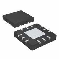
MAX9724AETC+ Maxim Integrated Products, MAX9724AETC+ Datasheet - Page 10

MAX9724AETC+
Manufacturer Part Number
MAX9724AETC+
Description
IC AMP AUDIO .045W STER 12TQFN
Manufacturer
Maxim Integrated Products
Series
DirectDrive™r
Type
Class ABr
Datasheet
1.MAX9724AETC.pdf
(19 pages)
Specifications of MAX9724AETC+
Output Type
Headphones, 2-Channel (Stereo)
Max Output Power X Channels @ Load
63mW x 2 @ 32 Ohm
Voltage - Supply
2.7 V ~ 5.5 V
Features
Depop, Short-Circuit and Thermal Protection, Shutdown
Mounting Type
Surface Mount
Package / Case
12-TQFN Exposed Pad
Product
General Purpose Audio Amplifiers
Output Power
42 mW
Thd Plus Noise
0.02 %
Supply Current
3.5 mA
Maximum Power Dissipation
1333 mW
Maximum Operating Temperature
+ 85 C
Mounting Style
SMD/SMT
Audio Load Resistance
16 Ohms
Minimum Operating Temperature
- 40 C
Amplifier Class
AB
No. Of Channels
2
Supply Voltage Range
2.7V To 5.5V
Load Impedance
16ohm
Operating Temperature Range
-40°C To +85°C
Amplifier Case Style
TQFN
Rohs Compliant
Yes
For Use With
MAX9724AEVKIT+ - EVALUATION KIT FOR MAX9724A/BMAX9724DEVKIT+ - KIT EVAL FOR MAX9724D
Lead Free Status / RoHS Status
Lead free / RoHS Compliant
the MAX9724 addresses the problem of the RF suscep-
tibility by rejecting RF noise and preventing it from cou-
pling into the audio band.
The RF susceptibility of an amplifier can be measured
by placing the amplifier in an isolated chamber and sub-
jecting it to an electric field of known strength. If the
electric field is modulated with an audio band signal, a
percentage of the modulated signal will be demodulat-
ed and amplified by the device in the chamber. Figure 2
shows the signal level at the outputs of an unoptimized
amplifier and the MAX9724. The test conditions are
shown in Table 1.
In conventional single-supply audio amplifiers, the out-
put-coupling capacitor contributes significantly to audi-
ble clicks and pops. Upon startup, the amplifier charges
the coupling capacitor to its bias voltage, typically half
the supply. Likewise, on shutdown, the capacitor is dis-
charged. This results in a DC shift across the capacitor,
which appears as an audible transient at the speaker.
Since the MAX9724A/ MAX9724B do not require output-
coupling capacitors, this problem does not arise.
Additionally, the MAX9724A/MAX9724B feature exten-
sive click-and-pop suppression that eliminates any audi-
ble transient sources internal to the device.
60mW, DirectDrive, Stereo Headphone Amplifier
with Low RF Susceptibility and Shutdown
Table 1. RF Susceptibility Test Conditions
Figure 2. RF Susceptibility of the MAX9724 and a Typical Headphone Amplifier
10
RF Field Strength
RF Modulation Type
RF Modulation Index
RF Modulation Frequency
______________________________________________________________________________________
TEST PARAMETER
Click-and-Pop Suppression
-100
-20
-40
-60
-80
40
20
0
100
MAX9724
62dB IMPROVEMENT
AT 850MHz
RF SUSCEPTIBLE
AMPLIFIER
Sine wave
SETTING
50V/m
100%
600
1kHz
RF CARRIER FREQUENCY (MHz)
39dB IMPROVEMENT
AT 900MHz
1100
67dB IMPROVEMENT
AT 1800MHz
1600
Typically, the output of the device driving the
MAX9724A/MAX9724B has a DC bias of half the supply
voltage. At startup, the input-coupling capacitor, C
charged to the preamplifier’s DC bias voltage through
the MAX9724A/MAX9724B input resistor, R
series 15kΩ resistor. This DC shift across the capacitor
results in an audible click-and-pop. Delay the rise of
SHDN 4 to 5 time constants based on R
to eliminate clicks-and-pops caused by the input filter.
The MAX9724A/MAX9724B feature a < 0.1µA, low-
power shutdown mode that reduces quiescent current
consumption and extends battery life for portable appli-
cations. Drive SHDN low to disable the amplifiers and
the charge pump. In shutdown mode, the amplifier out-
put impedance is set to 14kΩ||R
MAX9724B). The amplifiers and charge pump are
enabled once SHDN is driven high.
Under normal operating conditions, linear power ampli-
fiers can dissipate a significant amount of power. The
maximum power dissipation for each package is given
in the Absolute Maximum Ratings section under
Continuous Power Dissipation or can be calculated by
the following equation:
where T
ture, and θ
J(MAX)
49dB IMPROVEMENT
AT 1900MHz
2100
JA
P
DISSPKG MAX
is the reciprocal of the derating factor in
is +150°C, T
Applications Information
2600
(
)
=
A
T
is the ambient tempera-
J MAX
Power Dissipation
(
F
θ
(R
JA
)
F
−
T
IN
is 30kΩ for the
A
x 15kΩ x C
Shutdown
IN
, and a
IN
, is
IN


