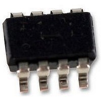
LTC2632ACTS8-HI12#PBF Linear Technology, LTC2632ACTS8-HI12#PBF Datasheet - Page 17

LTC2632ACTS8-HI12#PBF
Manufacturer Part Number
LTC2632ACTS8-HI12#PBF
Description
48T3782
Manufacturer
Linear Technology
Datasheet
1.LTC2632HTS8-HMI10TRPBF.pdf
(24 pages)
Specifications of LTC2632ACTS8-HI12#PBF
Resolution (bits)
12bit
Input Channel Type
Serial
Data Interface
3-Wire, Serial
Supply Voltage Range - Analog
4.5V To 5.5V
Supply Current
500µA
Digital Ic Case Style
TSOT-23
No. Of Pins
8
Rohs Compliant
Yes
Available stocks
Company
Part Number
Manufacturer
Quantity
Price
OPERATION
The LTC2632 is a family of dual voltage output DACs in an
8-lead TSOT package. Each DAC can operate rail-to-rail
using an external reference, or with its full-scale voltage
set by an integrated reference. Fifteen combinations of
accuracy (12-, 10-, and 8-bit), power-on reset value (zero-
scale, mid-scale in internal reference mode, or mid-scale
in external reference mode), and full-scale voltage (2.5V
or 4.096V) are available. The LTC2632 is controlled using
a 3-wire SPI/MICROWIRE compatible interface.
Power-On Reset
The LTC2632-HZ/LTC2632-LZ clear the output to zero-scale
when power is first applied, making system initialization
consistent and repeatable.
For some applications, downstream circuits are active
during DAC power-up, and may be sensitive to nonzero
outputs from the DAC during this time. The LTC2632 con-
tains circuitry to reduce the power-on glitch: the analog
output typically rises less than 10mV above zero-scale
during power-on if the power supply is ramped to 5V in
1ms or more. In general, the glitch amplitude decreases as
the power supply ramp time is increased. See “Power-On
Reset Glitch” in the Typical Performance Characteristics
section.
The LTC2632-HI/LTC2632-LI/LTC2632-LX provides an
alternative reset, setting the output to mid-scale when
power is first applied. The LTC2632-LI and LTC2632-HI
power-up in internal reference mode, with the output set
to a mid-scale voltage of 1.25V and 2.048V respectively.
The LTC2632-LX powers up in external reference mode,
with the output set to mid-scale of the external reference.
Default reference mode selection is described in the Refer-
ence Modes section.
Power Supply Sequencing
The voltage at REF (Pin 3) must be kept within the range
–0.3V ≤ V
Ratings section). Particular care should be taken to observe
these limits during power supply turn-on and turn-off
sequences, when the voltage at V
REF
≤ V
CC
+ 0.3V (see the Absolute Maximum
CC
is in transition.
Transfer Function
The digital-to-analog transfer function is
where k is the decimal equivalent of the binary DAC input
code, N is the resolution, and V
LI/LTC2632-LX/LTC2632-LZ) or 4.096V (LTC2632-HI/
LTC2632-HZ) when in internal reference mode, and the
voltage at REF when in external reference mode.
Table 1. Command Codes
COMMAND*
*Command codes not shown are reserved and should not be used.
Table 2. Address Codes
ADDRESS (n)*
* Address codes not shown are reserved and should not be used.
A3
C3
0
0
1
0
0
0
0
0
0
0
0
1
V
OUT(IDEAL)
C2
A2
0
0
0
0
1
1
1
1
1
0
0
1
C1
A1
0
0
1
1
0
0
1
1
1
0
0
1
=
C0
A0
0
1
0
1
0
1
0
1
1
0
1
1
2
DAC A
DAC B
All DACs
k
Write to Input Register n
Update (Power-Up) DAC Register n
Write to Input Register n, Update (Power-Up) All
Write to and Update (Power-Up) DAC Register n
Power-Down n
Power-Down Chip (All DAC’s and Reference)
Select Internal Reference (Power-Up Reference)
Select External Reference (Power-Down Internal
Reference)
No Operation
N
• V
REF
REF
is either 2.5V (LTC2632-
LTC2632
17
2632fa


