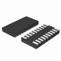
NCP2830MUTXG ON Semiconductor, NCP2830MUTXG Datasheet

NCP2830MUTXG
Specifications of NCP2830MUTXG
Related parts for NCP2830MUTXG
NCP2830MUTXG Summary of contents
Page 1
NCP2830 1W Constant Filterless Class-D Audio Amplifier NCP2830 is a cost effective mono audio power amplifier designed for portable communication device applications such as mobile phones. Due to its integrated charge pump structure, this part is capable of delivering 1 ...
Page 2
V C1P PVDD Lithium/ Ion Battery AVDD 2 x 4.7 mF, 0603 WM I/O from Microcontroller GS I/O from Microcontroller Shutdown and Biasing SD I/O from Microcontroller INM 1 mF INP 1 mF AGND Figure 2. Simplified ...
Page 3
PIN FUNCTION DESCRIPTION Pin Pin Name Type 20 VB_IN I This pin must be externally connection in a star configuration with Pin n°15. The C (10 mF/6.3 V/0603) capacitor must be connected as close as possible to the connection point. ...
Page 4
MAXIMUM RATINGS Rating AVDD, PVDD Pins: Power Supply Voltage (Note 2) Digital Input WM; SD; GS Pin: Human Body Model (HBM) ESD Rating are (Note 3) Machine Model (MM) ESD Rating are (Note 3) Latch up Current Maximum Rating QFN ...
Page 5
ELECTRICAL CHARACTERISTICS Min and Max Limits apply for T between 2 5.5 V (Unless otherwise noted). Typical values are referenced to T Symbol Parameter GLOBAL SYSTEM V Operating System Voltage DD I Shutdown Current SD I Shutdown Current ...
Page 6
ELECTRICAL CHARACTERISTICS Min and Max Limits apply for T between 2 5.5 V (Unless otherwise noted). Typical values are referenced to T Symbol Parameter CLASS D SECTION PSRR Power Supply Rejection Ratio CMRR Common mode rejection ratio h ...
Page 7
TYPICAL OPERATING CHARACTERISTICS −40°C 25°C 2 85°C 0 2.7 3.2 3.7 4.2 V (V) DD Figure Figure 5. VB Output Ripple 100 10 1 0.1 0.01 10 100 P P ...
Page 8
TYPICAL OPERATING CHARACTERISTICS 0 PSRR − 200 − −30 −40 −50 −60 −70 −80 −90 −100 −110 10 100 1000 FREQUENCY (Hz) Figure 9. PSRR vs Frequency 0 −10 PSRR ...
Page 9
TYPICAL OPERATING CHARACTERISTICS 7.E−05 No Filter 6.E−05 5.E−05 A Weighting 4.E−05 3.E−05 2.E−05 1.E− 0.E+00 3 100 1000 FREQUENCY (Hz) Figure 15. Noise vs Frequency High Low ...
Page 10
TYPICAL OPERATING CHARACTERISTICS − 12dB −20 −30 − −50 3.6 V −60 −70 −80 −90 −100 10 100 1000 FREQUENCY (Hz) Figure 21. CMRR vs Frequency 100 90 80 ...
Page 11
PVDD PVDD C1 4.7mF 0 WM VB_in AVDD ANALOG C2 4.7mF SD 0 AGND 0 GS INM 7.5k 7.5k INP 0 7.5k 7. Detailed Descriptions The NCP2830 consists of two parts: a DC−DC converter and a mono class ...
Page 12
V. Internally, the class D amplifier starts to operate when V equals 4 When VSD is low, the charge pump is deactivated and the V voltage is maintain to the shutdown mode ...
Page 13
Output Capacitors (C5 and C6) The value and ESR of this capacitor are directly linked to the ripple of the regulated output voltage. As the charge pump must provide up to 450 mA to the internal audio amplifier, two 10 ...
Page 14
... Digital Control INM Audio Inputs INP ORDERING INFORMATION Device NCP2830MUTXG †For information on tape and reel specifications, including part orientation and tape sizes, please refer to our Tape and Reel Packaging Specifications Brochure, BRD8011/D. TYPICAL APPLICATION 2.2 mF, 6.3 V 2.2 mF, 6 C1P C1N C2P C2N ...
Page 15
... A B NOTE 3 0.05 C *For additional information on our Pb−Free strategy and soldering details, please download the ON Semiconductor Soldering and Mounting Techniques Reference Manual, SOLDERRM/D. N. American Technical Support: 800−282−9855 Toll Free USA/Canada Europe, Middle East and Africa Technical Support: Phone: 421 33 790 2910 Japan Customer Focus Center Phone: 81− ...


